AZ12000K Ver la hoja de datos (PDF) - Arizona Microtek, Inc
Número de pieza
componentes Descripción
Fabricante
AZ12000K Datasheet PDF : 13 Pages
| |||
AZ12000
AZ12001
AZ12001 FUNCTIONAL PIN DESCRIPTIONS
Pin No
Pin Name
Functional Description
REFIN
Reference Crystal Resonator Input This pin includes an on-chip 470 Ω pull
down resistor to VBB. The input from the resonator circuit should be AC
coupled.
Crystal Resonator Output Drive This pin is an inverted and amplified version
of the signal on the REFIN pin. The gain from REFIN to R¯ E¯ ¯F¯O¯U¯ ¯T is
R¯ E¯ ¯F¯O¯U¯ ¯T
approximately 20. The IC includes a 4 ma on-chip current source. If more
current is needed, the R¯ E¯ ¯F¯O¯U¯ ¯T pin may be connected to VEE through a resistor
to provide up to 8 ma additional current.
Charge Pump Reference Output The pin voltage is nominally 1.2 volts below
CPREF
VCC. If an external integrator is used, CPREF should be connected to the
integrator reference input through a bias current cancellation network.
Charge Pump Output The charge pump output voltage is V(CPREF) ±0.3V
CPOUT
during a phase correction pulse. When there is no correction pulse the output
goes high impedance. If an external integrator is used, CPOUT should be
connected to the input integrator resistor.
Charge Pump Polarity Logic LOW on this pin causes CPOUT to go low
when the VCO frequency is too low, and go high when the VCO frequency is
too high. Logic HIGH on this pin causes CPOUT to go low when the VCO
CPPOL
frequency is too high, and go high when the VCO frequency is too low. This
pin should be LOW when the internal VCO is used.
INTREF
INTSUM
INTOUT
VCOSEL
If this pin is left open it is pulled to the HIGH condition.
Integrator Reference Input This pin should be connected to CPREF through a
bias current cancellation network
Integrator Summing Junction This pin is the summing junction for the
integrator amplifier
Integrator Output
Internal/External VCO Select Logic HIGH on this pin enables the internal
VCO. Logic LOW on this pin disables the internal VCO and allows use of the
EXTVCO inputs.
TANK
EXTVCO
E¯ ¯X¯T¯V¯ ¯C¯O¯
If this pin is left open it is pulled to the HIGH condition.
VCO Tank The tank components connect between this pin and VCC.
External VCO Input The external VCO input pins should be driven
differentially for best performance.
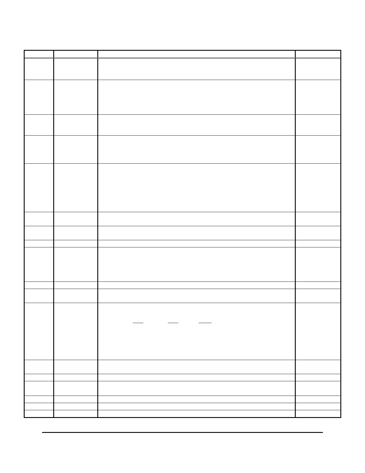
Divide Select VCO divide ratios are selected as shown:
DS2
DS1
Q
Q¯
N/C
VBB
VCC
VCOVCC
VEE
DS2
DS1
Ratio
LOW
LOW
÷4
LOW
HIGH
÷8
HIGH
LOW
÷16
HIGH
HIGH
÷32
If the pins are left open they are pulled to the HIGH condition.
Clock Output These pins are the main (multiplied) clock output.
No Connect This pin is used during factory test. It must be left open.
Reference Voltage Output This pin is used to bias the REFIN signal. It must
be bypassed externally to the VEE pins with a 0.01 µF capacitor.
Positive Supply +3.0 to +5.5 V
VCO Positive Supply +3.0 to +5.5 V
Negative Supply Ground
Logic Level
PECL
CMOS/TTL
compatible
CMOS/TTL
compatible
PECL
CMOS/TTL
Compatible
LVDS
January 2005 * REV - 3
www.azmicrotek.com
4
Share Link: 