AZ100ELT21 Ver la hoja de datos (PDF) - Arizona Microtek, Inc
Número de pieza
componentes Descripción
Fabricante
AZ100ELT21 Datasheet PDF : 5 Pages
| |||
AZ100ELT21
ARIZONA MICROTEK, INC.
Differential PECL to CMOS/TTL Translator
FEATURES
• Green / RoHS Compliant /
Lead (Pb) Free Package Available
• 3.5ns Typical Propagation Delay
• Differential PECL Inputs
• CMOS/TTL Outputs
• Flow Through Pinouts
• Operating Range of 3.0V to 5.5V
• Direct Replacement for
ON Semiconductor MC100ELT21
• Use AZ100ELT21 for 10K
Applications
DESCRIPTION
PACKAGE AVAILABILITY
PACKAGE
PART NO.
MARKING NOTES
AZM100
SOIC 8
AZ100ELT21D
ELT21
1,2
<Date Code>
SOIC 8 Green /
AZM100G
RoHS Compliant / AZ100ELT21DG
ELT21
1,2
Lead (Pb) Free
<Date Code>
TSSOP 8
AZ100ELT21T
AZH
T21
1,2
<Date Code>
TSSOP 8 Green /
AZHG
RoHS Compliant / AZ100ELT21TG
T21
1,2
Lead (Pb) Free
<Date Code>
1 Add R1 at end of part number for 7 inch (1K parts), R2 for 13 inch (2.5K parts)
Tape & Reel.
2 Date code format: “Y” for year followed by “WW” for week.
The AZ100ELT21 is a differential PECL to CMOS/TTL translator. Because PECL (Positive ECL) levels are
used, only VCC and ground are required. The small outline 8-lead packaging and the single gate of the ELT21 makes
it ideal for those applications where space, performance and low power are at a premium.
The ELT21 provides a VBB output for single-ended use or a DC bias reference for AC coupling to the device.
For single-ended input applications, the VBB reference should be connected to one side of the D0/D¯¯0 differential
input pair. The input signal is then fed to the other D0/D¯¯0 input. The VBB pin should be used only as a bias for the
ELT21 as its sink/source capability is limited. When used, the VBB pin should be bypassed to ground via a 0.01μF
capacitor.
NOTE: Specifications in the ECL/PECL tables are valid when thermal equilibrium is established.
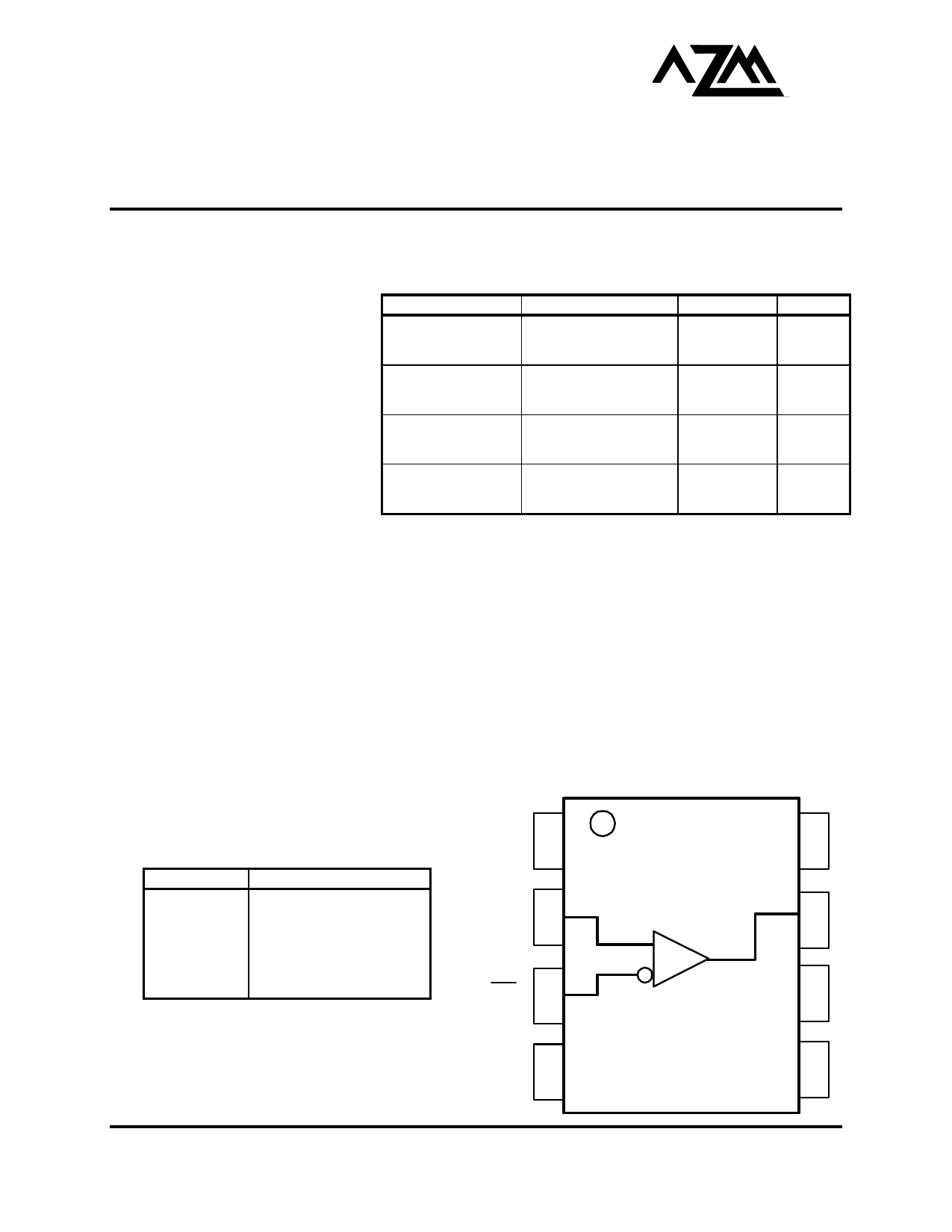
LOGIC DIAGRAM AND PINOUT ASSIGNMENT
PIN DESCRIPTION
PIN
Q
D0, D¯¯0
VCC
VBB
GND
NC
FUNCTION
CMOS/TTL Output
Differential Inputs
Positive Supply
Reference Voltage Output
Ground
No Connect
NC 1
D0 2
PECL
D0 3
8 VCC
CMOS/TTL
7Q
6 NC
VBB 4
5 GND
1630 S. STAPLEY DR., SUITE 127 • MESA, ARIZONA 85204 • USA • (480) 962-5881 • FAX (480) 890-2541
www.azmicrotek.com
Share Link: 