AWT6133M7P8 Ver la hoja de datos (PDF) - ANADIGICS
Número de pieza
componentes Descripción
Fabricante
AWT6133M7P8 Datasheet PDF : 8 Pages
| |||
AWT6133
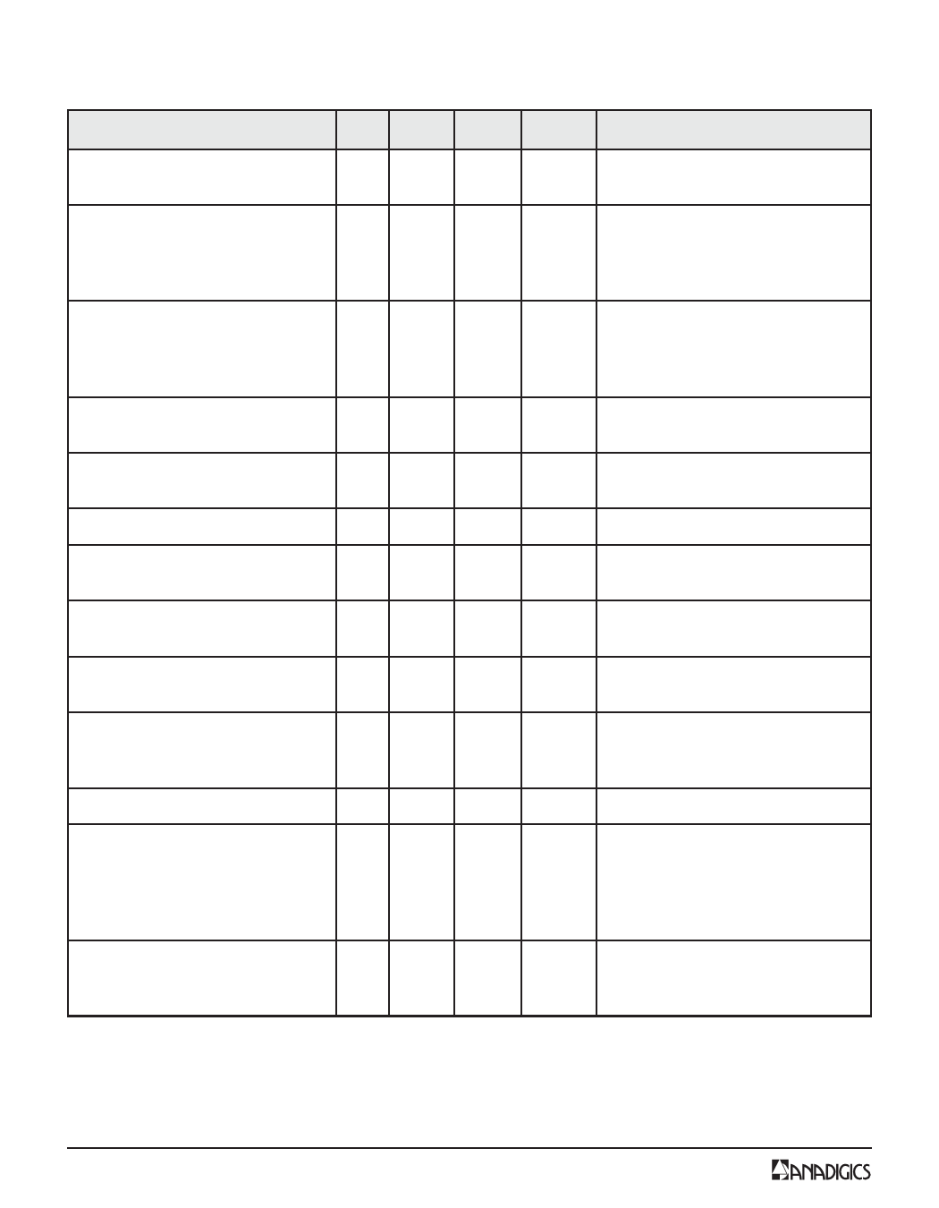
PARAMETER
Table 4: Electrical Specifications
(TC = +25 °C, VCC = +3.5 V, VREF = +2.85 V, 50 Ω system)
MIN TYP MAX UNIT
COMMENTS
Gain
25 27
30
22 24.5 27
Adjacent Channel Power (1)
at 61.25 MHz offset
Primary Channel BW = 1.23 MHZ -
-49
-47
Adjacent Channel BW = 30 kHz
-
-50
-47
Adjacent Channel Power
at 62.25 MHz offset
Primary Channel BW = 1.23 MHZ -
-60
-57
Adjacent Channel BW = 30 kHz
-
-65
-57
dB
POUT = +29 dBm, VMODE = 0 V
POUT = +16 dBm, VMODE = +2.85 V
dBc
POUT = +29 dBm, VMODE = 0 V
POUT = +16 dBm, VMODE = +2.85 V
dBc
POUT = +29 dBm, VMODE = 0 V
POUT = +16 dBm, VMODE = +2.85 V
Power-Added Efficiency (1)
Quiescent Current (Icq)
36 38
-
7.25 8
-
-
110 125
-
50
65
%
POUT = +29.5 dBm, VMODE = 0 V
POUT = +16 dBm, VMODE = +2.85 V
mA
VMODE = 0 V
VMODE = +2.85 V
Reference Current
-
3.7
5
mA through VREF pin, PA on
Mode Control Current
-
0.3
0.5
mA
through VMODE pin, VMODE = +2.85
V
Leakage Current
Noise in Receive Band
1930 MHz to 1990 MHz
-
<1
5
mA
VCC = +4.2 V, VREF = 0 V
VMODE = 0 V
- -136 -134 dBm/Hz
Harmonics
2fo
3fo, 4fo
-
-
-45
-30
-55
-30
dBc
Input Impedance
-
-
2:1 VSWR
Spurious Output Level
(all spurious outputs)
POUT [ +29 dBm
In-band load VSWR < 8:1
-
-
-65
dBc Out-of-band load VSWR 8:1
Applies over all voltage and
temperature operating ranges
Load mismatch stress with no
permanent degradation or failure
8:1
-
-
Notes:
(1) ACPR and PAE limits apply to middle frequency only.
VCC = +5.0 V, PIN = +5 dBm
VSWR Applies over full operating
temperature range
4
Data Sheet - Rev 2.0
12/2004
Share Link: 