AWT6123 Ver la hoja de datos (PDF) - ANADIGICS
Número de pieza
componentes Descripción
Fabricante
AWT6123 Datasheet PDF : 10 Pages
| |||
AWT6123
ELECTRICAL CHARACTERISTICS
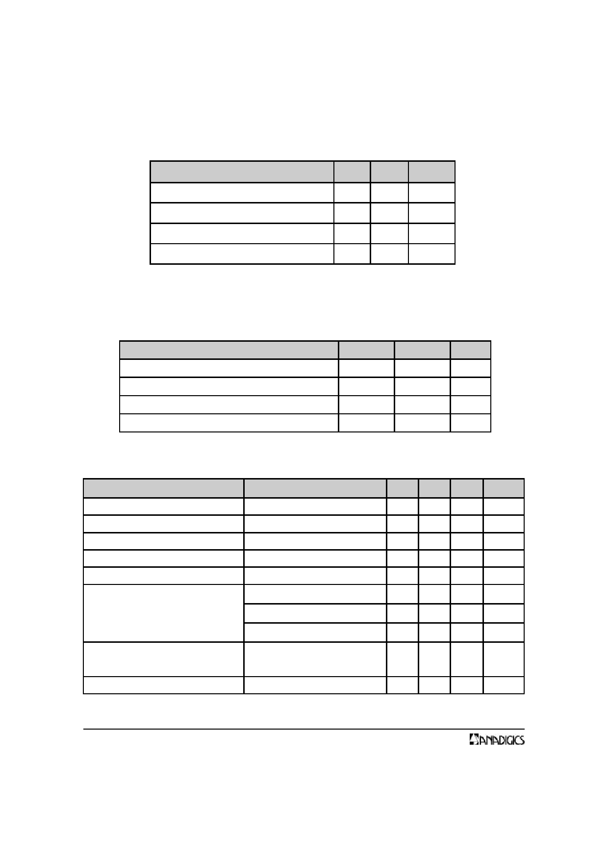
Table 1: Absolute Maximum Ratings
PARAMETER
MIN MAX UNITS
Supply Voltage (VCC)
+7
V
RF Input Power (RFIN)
+14 dBm
Control Voltage (VAPC)
3.0
V
Storage Temperature (TSTG)
-55 150
°C
Stresses in excess of the absolute ratings may cause permanent damage.
Functional operation is not implied under these conditions. Exposure to
absolute ratings for extended periods of time may adversely affect
reliability.
PARAMETER
Table 2: ESD Ratings
METHOD
ESD threshold voltage (RF ports)
HBM
ESD threshold voltage (control inputs)
HBM
ESD threshold voltage (RF inputs)
CDM
ESD threshold voltage (control inputs)
CDM
RATING
250
250
TBD
TBD
UNITS
V
V
V
V
Table 3: Operating Conditions
PARAMETER
CONDITIONS
Supply voltage (VCC)
Regulated voltage (VREG)
Individual Regulated current (IREG)
VREG_GSM or VREG_DCS/PCS = 3.0V
Control voltage (VAPC)
Control Voltage (VAPC) for max power
Individual Control current (IAPC)
See Note 1
VAPC = 0.45V
VAPC = 2.2V
VAPC = 3.0V
MIN TYP MAX UNITS
3.0 3.5 4.2
V
2.7 2.8 3.0
V
3.5 4.5
mA
0.45
VREG
V
1.8 2.2
V
-3
mA
3
mA
6
mA
Leakage current
VCC = 4.2V, No RF Applied
VREG_GSM = VREG_DCS/PCS = 0V
0
10
µA
Case temperature (TC)
-20
85
°C
Note 1: The VAPC must be pulled down to 0.45V with a low impedance. If VREG_GSM & VREG_DCS/PCS inputs
are connected then both VAPC inputs must be pulled down to 0.45V to disable both power amplifiers.
2
Advanced Product Information - Rev 0.7
02-2003
Share Link: 