AWT6109 Ver la hoja de datos (PDF) - ANADIGICS
Número de pieza
componentes Descripción
Fabricante
AWT6109 Datasheet PDF : 16 Pages
| |||
AWT6109
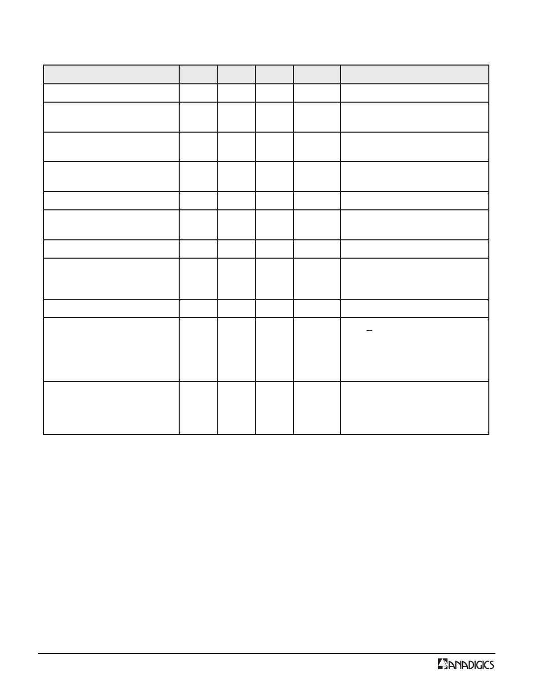
Table 4: Electrical Specifications
(TC = +25 °C, VCC = +3.5 V, VREF = +3.0 V, VMODE = +2.7 V, POUT = +28.5 dBm, 50Ω System)
PARAMETER
MIN TYP MAX UNIT
COMMENTS
Gain
Adjacent Channel Power
at ±1.25 MHz offset
Adjacent Channel Power
at ±2.25 MHz offset
Efficiency
Quiescent Current (Icq)
Leakage Current
(shutdown mode)
Noise in Receive Band
Harmonics
2fo
3fo, 4fo
Input Impedance
Spurious Output Level
(all spurious outputs)
Load mismatch stress with no
permanent degradation or
failure
27
30.5
32
-
-52.5 -46.5
-
-60
-57
31
35
-
6
7
-
50
65
85
dB
dB
Primary Channel BW = 1.23 MHz
Adjacent Channel BW = 30KHz
dB
Primary Channel BW = 1.23 MHz
Adjacent Channel BW = 30KHz
%
+28.5 dBm Output Power
+16 dBm Output Power
mA
<5
10
µA
VREF = 0 V, VMODE = 0 V
-
-136 -134 dBm/Hz 1840 MHz to 1870 MHz
-
-42
-30
dBc
-
-50
-30
-
-
2:1 VSWR
POUT < +29 dBm
In-band load VSWR < 8:1
-
-
-70
dBc Out-of-band load VSWR < 8:1
Applies over all voltage and
temperature operating ranges
8:1
-
VCC = +5.0 V
-
VSWR
PIN = +5 dBm
Applies over full operating
temperature range
4
Data Sheet - Rev 2.2
06/2002
Share Link: 