AWC6344P9 Ver la hoja de datos (PDF) - ANADIGICS
Número de pieza
componentes Descripción
Fabricante
AWC6344P9 Datasheet PDF : 8 Pages
| |||
AWC6344
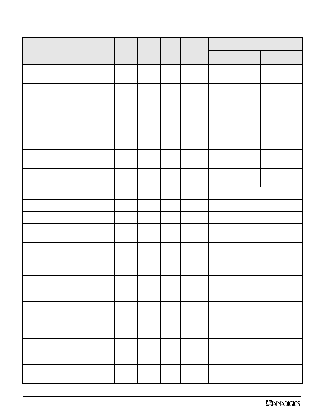
Table 4: Electrical Specifications - CDMA Operation (CDMA2000, RC-1 waveform)
(TC = +25 °C, VBATT = VCC = +3.4 V, VENABLE = +1.8 V, 50 Ω system)
PARAMETER
COMMENTS
MIN TYP MAX UNIT
POUT
VMODE
Gain
24 26.5 30
17
20
23
dB
POUT = +28 dBm 0 V
POUT = +16.5 dBm 1.8 V
Adjacent Channel Power
at +1.25 MHz offset
-
-51 -46
POUT = +28 dBm 0 V
Primary Channel BW - 1.23 MHz
-
-53 -46
dBc POUT = +16.5 dBm 1.8 V
Adjacent Channel BW = 30 kHz
Adjacent Channel Power
at +1.98 MHz
Primary Channel BW=1.23 MHz
Adjacent Channel BW=30 kHz
-
-55 -53
POUT = +28 dBm 0 V
-
-56 -53
dBc POUT = +16.5 dBm 1.8 V
Efficiency
33.5 37
-
29
34
-
%
POUT = +28 dBm 0 V
POUT = +16.5 dBm 1.8 V
Quiescent Current (Icq)
Low Bias Mode
-
9
14
mA through VCC pin 1.8 V
Mode Control Current
-
3.5 4.5
mA through VMODE pin, VMODE = +1.8 V
Enable Current
-
0.04 0.1
mA through VEN pin
BATT Current
-
0.8 1.5
mA through VBATT pin, VMODE = +1.8 V
Leakage Current
-
<5
10
µA
VBATT = +4.35 V, VCC = +4.35 V
VEN = 0 V, VMODE = 0 V
Noise Power
-
-141 -138
2110 MHz to 2155 MHz
-
-
-134
-134
-
-
dBm/Hz
1805 MHz to 1880 MHz
GPS Band
-
-145
-
ISM Band
Harmonics
2fo
4fo
-
-44 -35
dBc POUT ≤ +28 dBm
-
-55 -42
Coupling Factor
-
20.5
-
dB
Directivity
-
20
-
dB
Daisy Chain Insertion Loss
-
0.25
-
dB
Spurious Output Level
(all spurious outputs)
POUT < +28 dBm, In-Band VSWR
-
-
-70
dBc <5:1, Out-Of-Band VSWR< 10:1
Applies to all operating conditions
Load mismatch stress with no
permanent degradation or failure
8:1
-
-
VSWR
Notes:
(1) ACLR and Efficiency limits are applied at mid-band.
4
DATA SHEET - Rev 2.2
11/2012
Applies over full operating range
Share Link: 