AWC6323 Ver la hoja de datos (PDF) - ANADIGICS
Número de pieza
componentes Descripción
Fabricante
AWC6323 Datasheet PDF : 11 Pages
| |||
AWC6323
ELECTRICAL CHARACTERISTICS
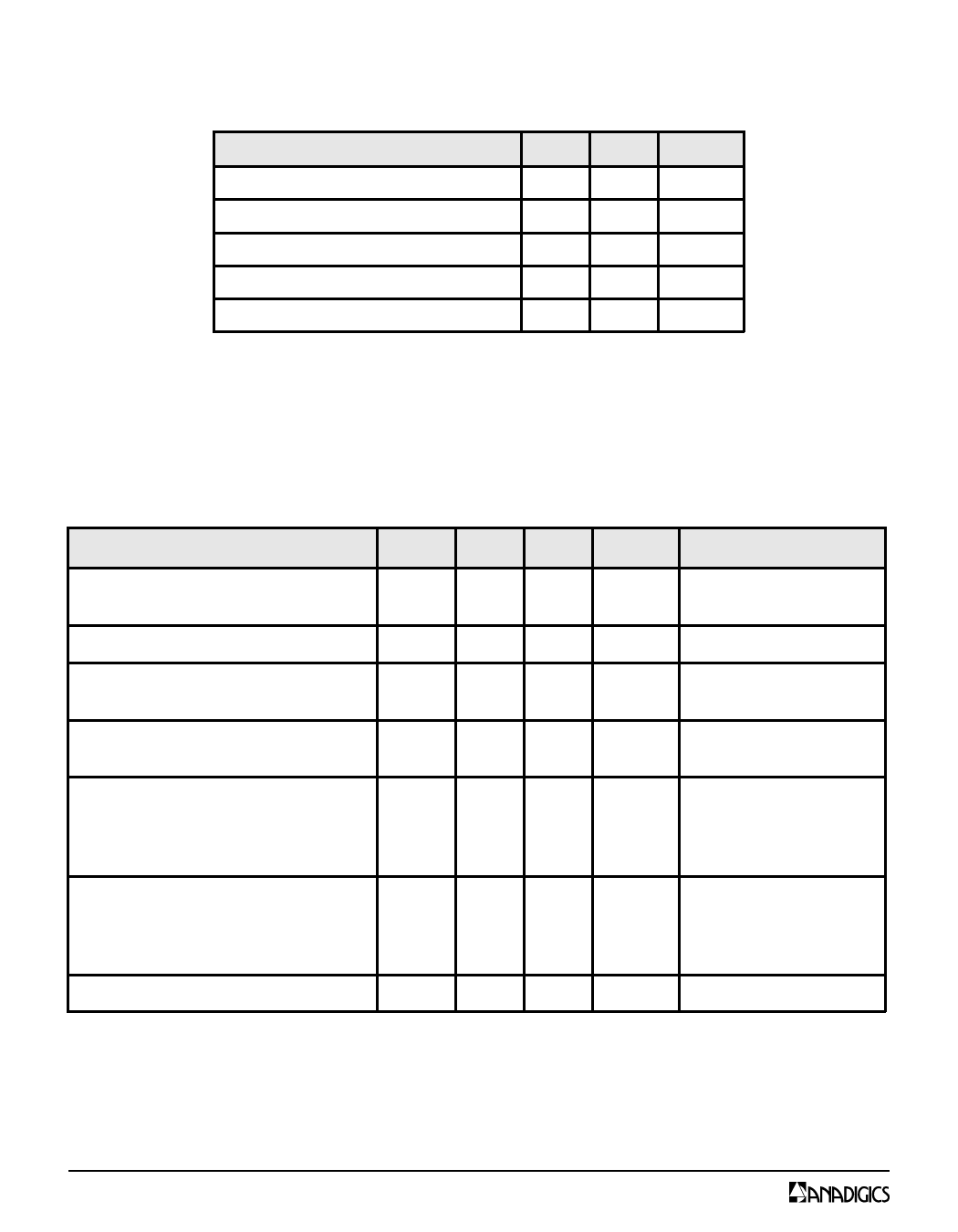
Table 2: Absolute Minimum and Maximum Ratings
PARAMETER
MIN MAX UNIT
Supply Voltage (VBATT, VCC, VCCA)
0
+5
V
Mode Control Voltage (VMODE1, VMODE2)
0
+3.5
V
Enable Voltage (VEN_CELL, VEN_PCS)
0
+3.5
V
RF Input Power (PIN)
-
+10
dBm
Storage Temperature (TSTG)
-40 +150
°C
Stresses in excess of the absolute ratings may cause permanent damage.
Functional operation is not implied under these conditions. Exposure
to absolute ratings for extended periods of time may adversely affect
reliability.
PARAMETER
Table 3: Operating Ranges
MIN TYP MAX
UNIT
COMMENTS
Operating Frequency (f)
824
1850
-
849
1910
MHz
Cellular
PCS
Supply Voltage (VCC and VBATT)
+3.2 +3.4 +4.2
V
Enable Voltage (VEN)
+1.35 +1.8 +3.1
0
-
+0.5
V
PA "on"
PA "shut down"
Mode Control Voltage (VMODE1, VMODE2)
+1.35 +1.8 +3.1
0
-
+0.5
V
High State Voltage
Low State Voltage
Cellular RF Output Power (POUT)
CDMA, HPM
CDMA, MPM
CDMA, LPM
+27.1 (1) 27.6
-
-
16
-
-
10
-
dBm CDMA 2000, RC-1
PCS RF Output Power (POUT)
CDMA, HPM
CDMA, MPM
CDMA, LPM
+27.4 (1) +27.9
-
-
16
-
-
10
-
dBm CDMA 2000, RC-1
Case Temperature (TC)
-30
-
+90
°C
The device may be operated safely over these conditions; however, parametric performance is guaranteed only
over the conditions defined in the electrical specifications.
Notes:
(1) For operation at VCC = +3.2 V, POUT is derated by 0.5 dB.
3
Data Sheet - Rev 2.2
03/2012
Share Link: 