ATTINY2313V Ver la hoja de datos (PDF) - Atmel Corporation
NГәmero de pieza
componentes DescripciГіn
Fabricante
ATTINY2313V Datasheet PDF : 226 Pages
| |||
Stack Pointer
ATtiny2313
The Stack is mainly used for storing temporary data, for storing local variables and for storing
return addresses after interrupts and subroutine calls. The Stack Pointer Register always points
to the top of the Stack. Note that the Stack is implemented as growing from higher memory loca-
tions to lower memory locations. This implies that a Stack PUSH command decreases the Stack
Pointer.
The Stack Pointer points to the data SRAM Stack area where the Subroutine and Interrupt
Stacks are located. This Stack space in the data SRAM must be defined by the program before
any subroutine calls are executed or interrupts are enabled. The Stack Pointer must be set to
point above 0x60. The Stack Pointer is decremented by one when data is pushed onto the Stack
with the PUSH instruction, and it is decremented by two when the return address is pushed onto
the Stack with subroutine call or interrupt. The Stack Pointer is incremented by one when data is
popped from the Stack with the POP instruction, and it is incremented by two when data is
popped from the Stack with return from subroutine RET or return from interrupt RETI.
The AVR Stack Pointer is implemented as two 8-bit registers in the I/O space. The number of
bits actually used is implementation dependent. Note that the data space in some implementa-
tions of the AVR architecture is so small that only SPL is needed. In this case, the SPH Register
will not be present.
Bit
Read/Write
Initial Value
15
вҖ“
SP7
7
R
R/W
RAMEND
RAMEND
14
вҖ“
SP6
6
R
R/W
RAMEND
RAMEND
13
вҖ“
SP5
5
R
R/W
RAMEND
RAMEND
12
вҖ“
SP4
4
R
R/W
RAMEND
RAMEND
11
вҖ“
SP3
3
R
R/W
RAMEND
RAMEND
10
вҖ“
SP2
2
R
R/W
RAMEND
RAMEND
9
вҖ“
SP1
1
R
R/W
RAMEND
RAMEND
8
вҖ“
SP0
0
R
R/W
RAMEND
RAMEND
SPH
SPL
Instruction
Execution Timing
This section describes the general access timing concepts for instruction execution. The AVR
CPU is driven by the CPU clock clkCPU, directly generated from the selected clock source for the
chip. No internal clock division is used.
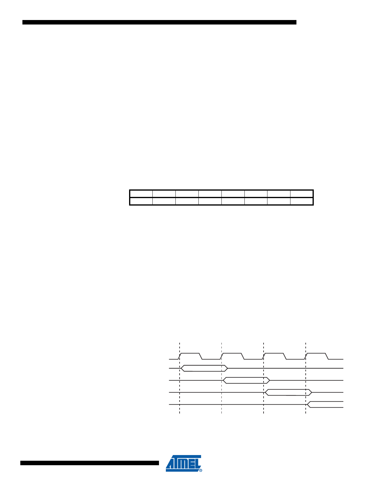
Figure 6 shows the parallel instruction fetches and instruction executions enabled by the Har-
vard architecture and the fast-access Register File concept. This is the basic pipelining concept
to obtain up to 1 MIPS per MHz with the corresponding unique results for functions per cost,
functions per clocks, and functions per power-unit.
Figure 6. The Parallel Instruction Fetches and Instruction Executions
T1
T2
T3
T4
clkCPU
1st Instruction Fetch
1st Instruction Execute
2nd Instruction Fetch
2nd Instruction Execute
3rd Instruction Fetch
3rd Instruction Execute
4th Instruction Fetch
2543LвҖ“AVRвҖ“08/10
Figure 7 shows the internal timing concept for the Register File. In a single clock cycle an ALU
operation using two register operands is executed, and the result is stored back to the destina-
tion register.
11
Share Link: 