ATA2516 Ver la hoja de datos (PDF) - Atmel Corporation
Número de pieza
componentes Descripción
Fabricante
ATA2516 Datasheet PDF : 10 Pages
| |||
ATA2516
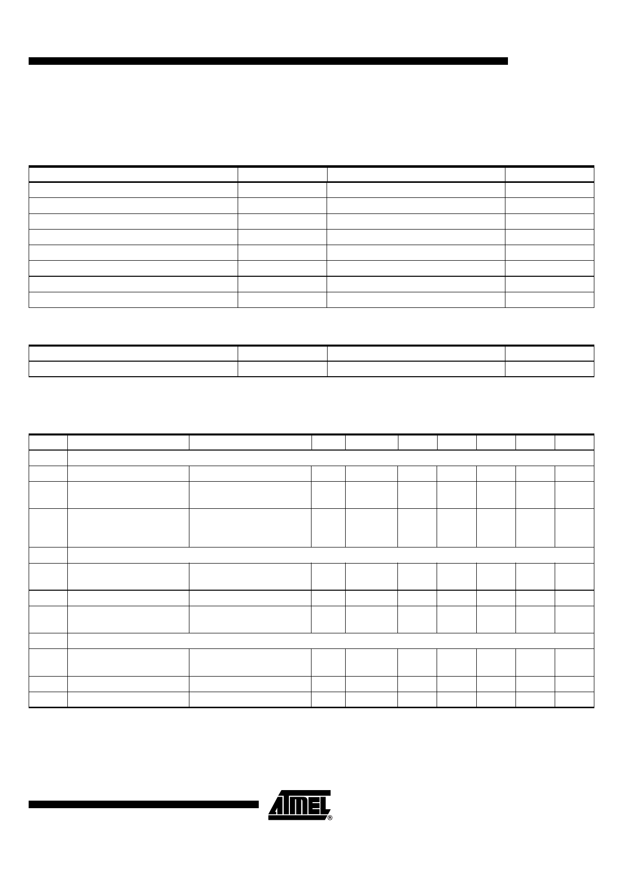
Absolute Maximum Ratings
Stresses beyond those listed under “Absolute Maximum Ratings” may cause permanent damage to the device. This is a stress rating
only and functional operation of the device at these or any other conditions beyond those indicated in the operational sections of this
specification is not implied. Exposure to absolute maximum rating conditions for extended periods may affect device reliability.
Parameters
Symbol
Value
Unit
Supply voltage
VS
-0.3 to 6
V
Supply current (DC current IIN_DC = 0)
IS
0.5
mA
Input voltage
VIN
-0.3 to VS
V
Input DC current at VS = 5 V
IIN_DC
0.8
mA
Output voltage
VO
-0.3 to VS
V
Operating temperature
Tamb
-40 to +85
°C
Storage temperature
Tstg
-40 to +125
°C
Power dissipation at Tamb = 25°C
Ptot
10
mW
Thermal Resistance
Parameters
Junction ambient TSSOP8
Symbol
RthJA
Value
TBD
Unit
K/W
Electrical Characteristics
Tamb = 25°C, VS = 5 V unless otherwise specified.
No. Parameters
Test Conditions
Pin Symbol Min. Typ. Max. Unit Type*
1 Supply
1.1 Supply-voltage range
1.2 Supply current
IIN_DC = 0; see
Figure 6 on page 7
1
VS
4.5
5
5.5
V
C
1
IS
0.29 0.34 mA
A
1.3 Supply current
2 Output
IIN_DC = 0; see
Figure 6 on page 7
Tamb = -40°C to 85°C
1
IS
0.4
mA
B
2.1 Internal pull-up resistor
Tamb = 25°C; see
Figure 3 on page 5
1, 3
RPU
65
100 135
kΩ
A
2.2 Output voltage low
2.3 Output voltage high
RLoad = 2.4 kΩ
3, 6
VOL
100
250
mV
A
3, 1
VOH
VS -
0.25
VS
V
A
3 Input
3.1
Maximum input DC current
VIN = 0; see
Figure 8 on page 7
5
IIN_DCMAX
580
760
µA
A
3.2 Maximum input DC current VIN = 0; Tamb = 85°C
3.3 Number of pulses required
5
IIN_DCMAX
490
650
5
6
µA
C
A
*) Type means: A =100% tested, B = 100% correlation tested, C = Characterized on samples, D = Design parameter
Note: BER = bit error rate; e.g. BER = 5% means that with P = 20 at the input pins 19 to 21, pulses may appear at the OUT pin.
3
4801B–AUTO–10/04
Share Link: 