AT49F004 Ver la hoja de datos (PDF) - Atmel Corporation
Número de pieza
componentes Descripción
Fabricante
AT49F004 Datasheet PDF : 15 Pages
| |||
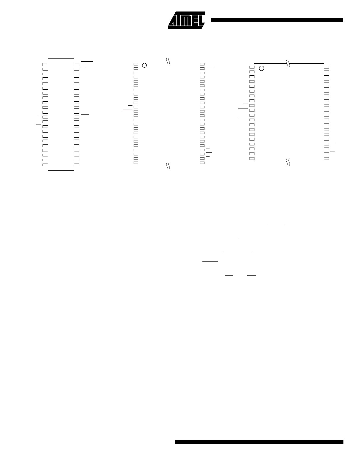
AT49F4096A(T) SOIC (SOP)
NC 1
NC 2
A17 3
A7 4
A6 5
A5 6
A4 7
A3 8
A2 9
A1 10
A0 11
CE 12
GND 13
OE 14
I/O0 15
I/O8 16
I/O1 17
I/O9 18
I/O2 19
I/O10 20
I/O3 21
I/O11 22
44 RESET
43 WE
42 A8
41 A9
40 A10
39 A11
38 A12
37 A13
36 A14
35 A15
34 A16
33 BYTE
32 GND
31 I/O15/A-1
30 I/O7
29 I/O14
28 I/O6
27 I/O13
26 I/O5
25 I/O12
24 I/O4
23 VCC
AT49F4096A(T) TSOP Top View
Type 1
A15 1
A14 2
A13 3
A12 4
A11 5
A10 6
A9 7
A8 8
NC 9
NC 10
WE 11
RESET 12
NC 13
NC 14
NC 15
NC 16
A17 17
A7 18
A6 19
A5 20
A4 21
A3 22
A2 23
A1 24
48 A16
47 BYTE
46 GND
45 I/O15 / A-1
44 I/O7
43 I/O14
42 I/O6
41 I/O13
40 I/O5
39 I/O12
38 I/O4
37 VCC
36 I/O11
35 I/O3
34 I/O10
33 I/O2
32 I/O9
31 I/O1
30 I/O8
29 I/O0
28 OE
27 GND
26 CE
25 A0
AT49F004(T) TSOP Top View
Type 1
A16 1
A15 2
A14 3
A13 4
A12 5
A11 6
A9 7
A8 8
WE 9
RESET 10
NC 11
RDY/BUSY 12
A18 13
A7 14
A6 15
A5 16
A4 17
A3 18
A2 19
A1 20
40 A17
39 GND
38 NC
37 NC
36 A10
35 I/O7
34 I/O6
33 I/O5
32 I/O4
31 VCC
30 VCC
29 NC
28 I/O3
27 I/O2
26 I/O1
25 I/O0
24 OE
23 GND
22 CE
21 A0
block of data and then programming on a byte-by-byte or
word-by-word basis.
The device is erased by executing the erase command
sequence; the device internally controls the erase opera-
tion. The memory is divided into four blocks for erase oper-
ations. There are two 4K word parameter block sections,
the boot block, and the main memory array block. The typi-
cal number of program and erase cycles is in excess of
10,000 cycles.
The 8K word boot block section includes a reprogramming
lock out feature to provide data integrity. This feature is
enabled by a command sequence. Once the boot block
programming lockout feature is enabled, the data in the
boot block cannot be changed when input levels of 5.5
volts or less are used. The boot sector is designed to con-
tain user secure code.
For the AT49F4096A(T), the BYTE pin controls whether
the device data I/O pins operate in the byte or word config-
uration. If the BYTE pin is set at a logic “1” or left open, the
device is in word configuration, I/O0 - I/O15 are active and
controlled by CE and OE.
If the BYTE pin is set at logic “0”, the device is in byte con-
figuration, and only data I/O pins I/O0 - I/O7 are active and
controlled by CE and OE. The data I/O pins I/O8 - I/O14
are tri-stated and the I/O15 pin is used as an input for the
LSB (A-1) address function.
2
AT49F004(T)/4096A(T)
Share Link: 