AT25DF321A Ver la hoja de datos (PDF) - Atmel Corporation
Número de pieza
componentes Descripción
Fabricante
AT25DF321A Datasheet PDF : 51 Pages
| |||
Atmel AT25DF321A
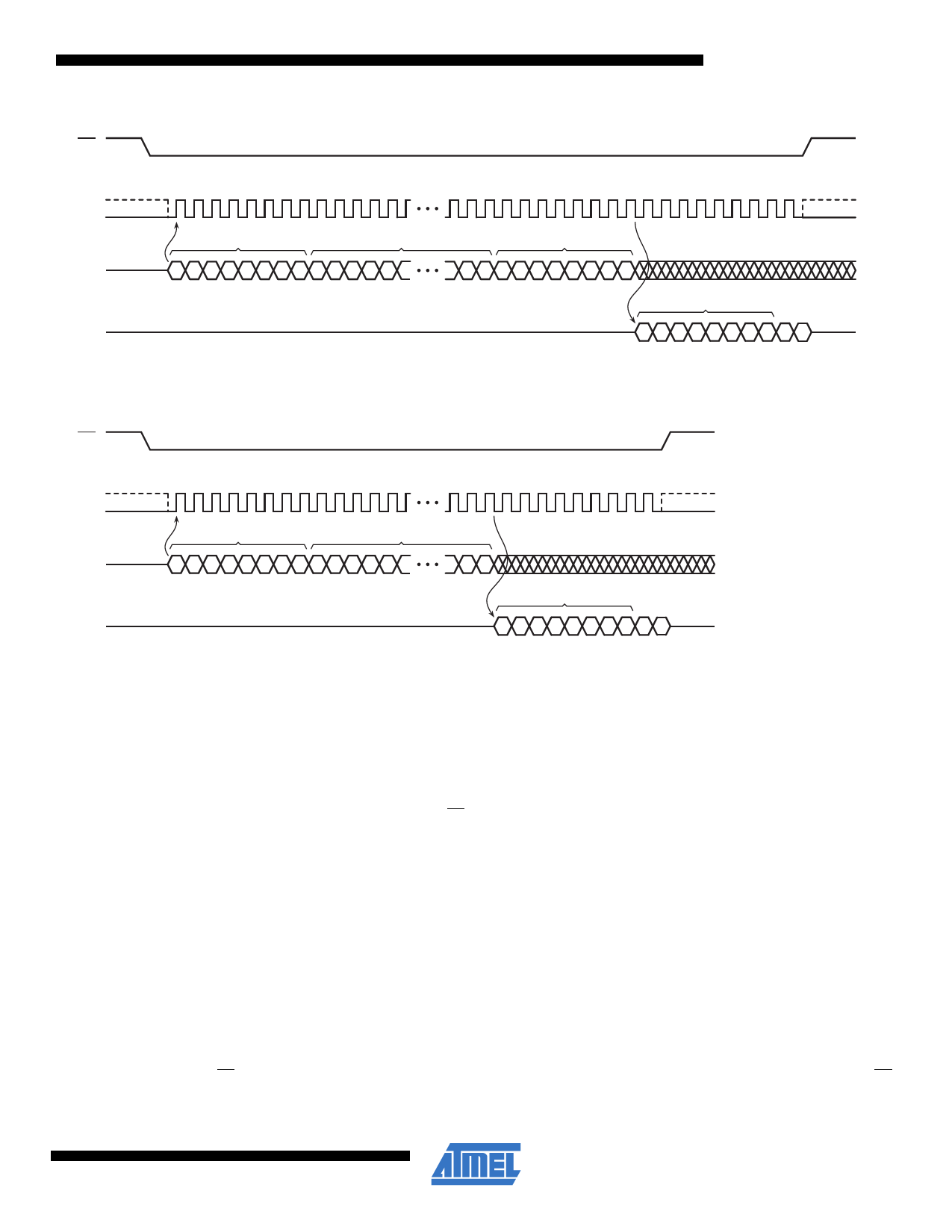
Figure 7-2.
CS
Read Array – 0Bh Opcode
SCK
SI
SO
0 1 2 3 4 5 6 7 8 9 10 11 12
29 30 31 32 33 34 35 36 37 38 39 40 41 42 43 44 45 46 47 48
OPCODE
ADDRESS BITS A23-A0
DON'T CARE
0 0 0 0 1 0 1 1AAAAAA
MSB
MSB
HIGH-IMPEDANCE
AAAXXXXXXXX
MSB
DATA BYTE 1
DDDDDDDDDD
MSB
MSB
Figure 7-3.
CS
Read Array – 03h Opcode
SCK
SI
SO
0 1 2 3 4 5 6 7 8 9 10 11 12
29 30 31 32 33 34 35 36 37 38 39 40
OPCODE
ADDRESS BITS A23-A0
0 0 0 0 0 0 1 1AAAAAA
MSB
MSB
HIGH-IMPEDANCE
AAA
DATA BYTE 1
DDDDDDDDDD
MSB
MSB
7.2 Dual-Output Read Array
The Dual-Output Read Array command is similar to the standard Read Array command and can be used to sequentially
read a continuous stream of data from the device by simply providing the clock signal once the initial starting address has
been specified. Unlike the standard Read Array command, however, the Dual-Output Read Array command allows two
bits of data to be clocked out of the device on every clock cycle rather than just one.
The Dual-Output Read Array command can be used at any clock frequency up to the maximum specified by fRDDO. To
perform the Dual-Output Read Array operation, the CS pin must first be asserted and the opcode of 3Bh must be clocked
into the device. After the opcode has been clocked in, the three address bytes must be clocked in to specify the starting
address location of the first byte to read within the memory array. Following the three address bytes, a single dummy byte
must also be clocked into the device.
After the three address bytes and the dummy byte have been clocked in, additional clock cycles will result in data being
output on both the SO and SIO pins. The data is always output with the MSB of a byte first, and the MSB is always output
on the SO pin. During the first clock cycle, bit 7 of the first data byte will be output on the SO pin while bit 6 of the same
data byte will be output on the SIO pin. During the next clock cycle, bits 5 and 4 of the first data byte will be output on the
SO and SIO pins, respectively. The sequence continues with each byte of data being output after every four clock cycles.
When the last byte (3FFFFFh) of the memory array has been read, the device will continue reading back at the beginning
of the array (000000h). No delays will be incurred when wrapping around from the end of the array to the beginning of
the array.
Deasserting the CS pin will terminate the read operation and put the SO and SIO pins into a high-impedance state. The CS
pin can be deasserted at any time and does not require that a full byte of data be read.
9
3686D–DFLASH–12/09
Share Link: 