AT25DF081A Ver la hoja de datos (PDF) - Atmel Corporation
Número de pieza
componentes Descripción
Fabricante
AT25DF081A Datasheet PDF : 53 Pages
| |||
7. Read Commands
7.1 Read Array
The Read Array command can be used to sequentially read a continuous stream of data from the device by simply
providing the clock signal once the initial starting address has been specified. The device incorporates an internal
address counter that automatically increments on every clock cycle.
Three opcodes (1Bh, 0Bh, and 03h) can be used for the Read Array command. The use of each opcode depends
on the maximum clock frequency that will be used to read data from the device. The 0Bh opcode can be used at
any clock frequency up to the maximum specified by fCLK, and the 03h opcode can be used for lower frequency
read operations up to the maximum specified by fRDLF. The 1Bh opcode allows the highest read performance pos-
sible and can be used at any clock frequency up to the maximum specified by fMAX; however, use of the 1Bh
opcode at clock frequencies above fCLK should be reserved to systems employing the Atmel RapidSTM protocol.
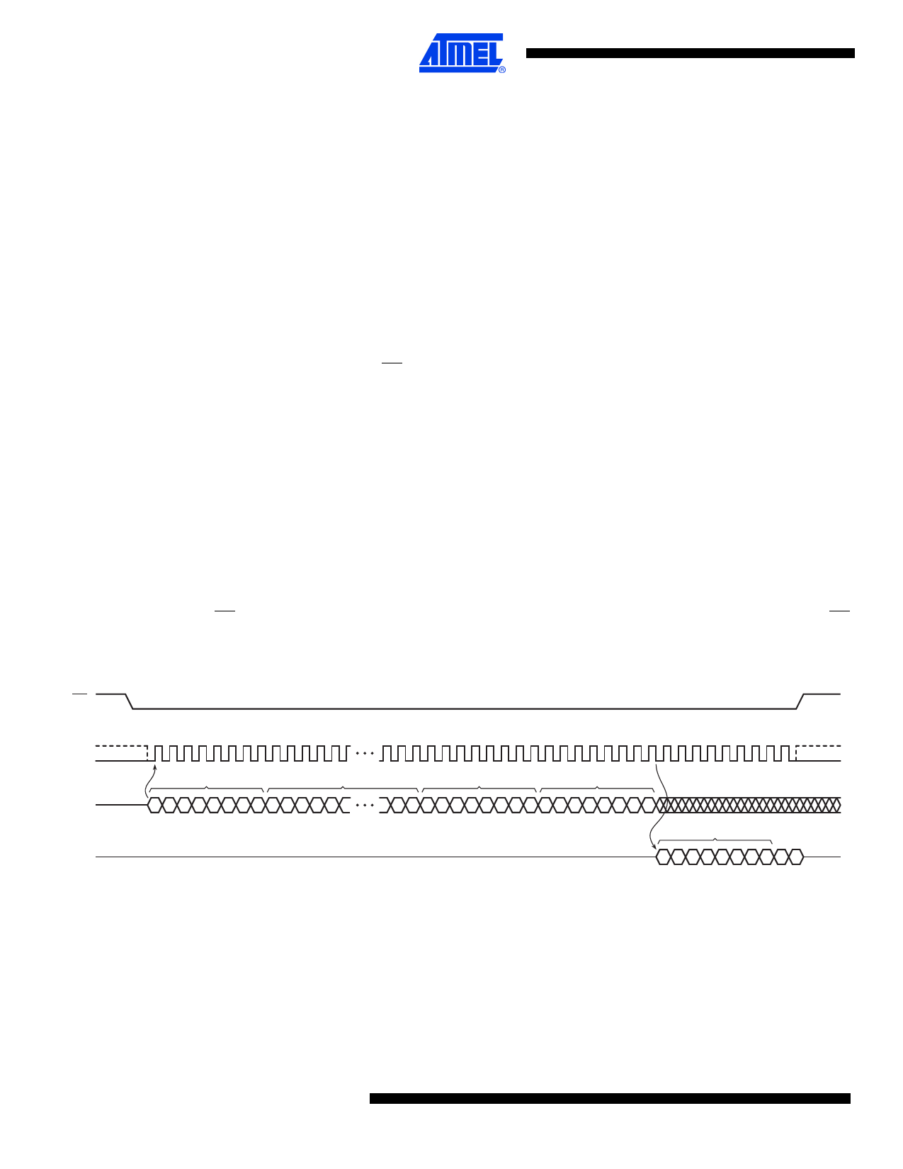
To perform the Read Array operation, the CS pin must first be asserted and the appropriate opcode (1Bh, 0Bh, or
03h) must be clocked into the device. After the opcode has been clocked in, the three address bytes must be
clocked in to specify the starting address location of the first byte to read within the memory array. Following the
three address bytes, additional dummy bytes may need to be clocked into the device depending on which opcode
is used for the Read Array operation. If the 1Bh opcode is used, then two dummy bytes must be clocked into the
device after the three address bytes. If the 0Bh opcode is used, then a single dummy byte must be clocked in after
the address bytes.
After the three address bytes (and the dummy bytes or byte if using opcodes 1Bh or 0Bh) have been clocked in,
additional clock cycles will result in data being output on the SO pin. The data is always output with the MSB of a
byte first. When the last byte (0FFFFFh) of the memory array has been read, the device will continue reading back
at the beginning of the array (000000h). No delays will be incurred when wrapping around from the end of the array
to the beginning of the array.
Deasserting the CS pin will terminate the read operation and put the SO pin into a high-impedance state. The CS
pin can be deasserted at any time and does not require that a full byte of data be read.
Figure 7-1. Read Array – 1Bh Opcode
CS
SCK
SI
SO
0 1 2 3 4 5 6 7 8 9 10 11 12
29 30 31 32 33 34 35 36 37 38 39 40 41 42 43 44 45 46 47 48 49 50 51 52 53 54 55 56
OPCODE
ADDRESS BITS A23-A0
DON'T CARE
DON'T CARE
0 0 0 1 1 0 1 1AAAAAA
MSB
MSB
HIGH-IMPEDANCE
AAAXXXXXXXXXXXXXXXX
MSB
MSB
DATA BYTE 1
DDDDDDDDDD
MSB
MSB
8 Atmel AT25DF081A
8715B–SFLSH–8/10
Share Link: 