NX25F641C Ver la hoja de datos (PDF) - NexFlash -> Winbond Electronics
Número de pieza
componentes Descripción
Fabricante
NX25F641C Datasheet PDF : 23 Pages
| |||
NX25F641C
Pin Descriptions
Serial Data Input (SI)
The SI pin receives data into the device with the SCK pin.
All data transmitted to the device is clocked relative to the
rising edge of SCK.
Serial Data Output (SO)
The SO pin transmits data from the device with the SCK
pin. All data transmitted from the device is clocked relative
to the edge defined with the RCE bit in the configuration
register. The default is RCE bit set to 0 which outputs data
on the falling edge of the SCK pin and is compatible with
standard systems that support SPI. The clock rate can be
faster with the SPI_RCE bit set to 1, (see tCYC in AC
Characteristics).
Serial Clock Input (SCK)
All commands and data written to the SI pin are clocked
relative to rising edge of SCK. All data read from the SO
pin is clocked relative to the rising or falling edge of SCK.
Chip Select (CS)
The chip select input is required to start and finish an SPI
command. SCK must be low when chip select is asserted
low. Upon power-up, an initial low-high transition of chip
select is required before any command will be acknowl-
edged. Once the device is de-selected, the SO pin will
enter a high impedance state and power consumption will
be reduced to standby levels unless a transfer, compare,
or sector programming are in progress. If a transfer,
compare, or sector programming is in progress, the
command will complete and then the device will enter
standby mode.
Write Protect Input (WP)
The write protect input (WP) works in conjunction with the
configuration register bits WR3..WR0, WD, and the status
register bit WE. When WP is asserted low, the entire flash
memory array is write protected. When the WP pin is high
and the status register WE bit set, the device addresses
corresponding to the write protect range and direction are
write protected. When the status register bit WE is reset,
the entire array is write protected. See the section on the
configuration register for more details.
HOLD , Ready/Busy or No-connect
(HOLD, R/B or N/C)
This multifunction pin can serve either as a Hold input
(HOLD), Ready/Busy output (Ready-/Busy or a
No-connect). The pin function is user programmable
through the configuration register bits HR0, HR1. The
device comes from the factory with this pin
programmed as a No Connect (NC). The pin can be
re-configured by the user by writing to the configuration
register.
Power Supply Pins (Vcc and Gnd)
The NX25F641C supports a single power supply between
2.7V and 3.6V connected to the Vcc and Gnd pins.
HOLD-R/B
1
NC 2
WP
3
NC 4
NC 5
NC 6
VCC 7
GND 8
NC 9
NC 10
NC 11
CS
12
NC 13
SCK 14
SI 15
SO 16
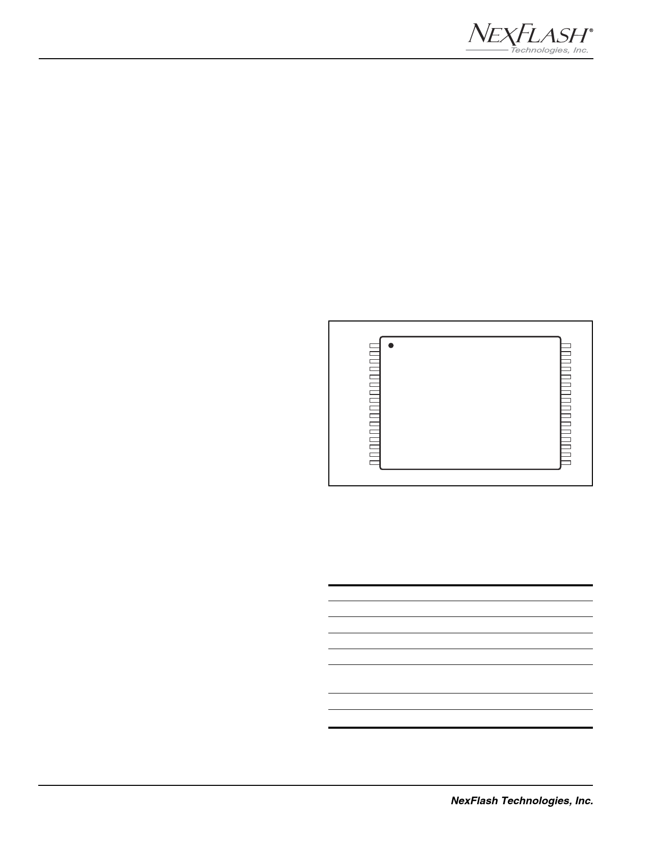
32-PIN TSOP (Type I)
NX25F641C
SPI Interface
32
NC
31
NC
30
NC
29
NC
28
NC
27
NC
26
NC
25
NC
24
NC
23
NC
22
NC
21
NC
20
NC
19
NC
18
NC
17
NC
Figure 2. NX25F641C Pin Assignments
SPI Interface, 32-Pin TSOP, Type I (T Package)
Table 1. Pin Descriptions for the 25F641C
SI
SO
SCK
CS
WP
Hold, R/B
VCC
GND
Serial Data Input
Serial Data Output
Serial Clock Input
Chip Select Input
Write Protect Input
Hold Input Ready-Busy Output or
No Connect
Power Supply
Ground
6
NexFlash Technologies, Inc.
PRELIMINARY NXSF032A-0502
05/06/02 ©
Share Link: 