NX26F640C-3T-R Ver la hoja de datos (PDF) - NexFlash -> Winbond Electronics
Número de pieza
componentes Descripción
Fabricante
NX26F640C-3T-R Datasheet PDF : 23 Pages
| |||
NX26F640C
Write Protection
The NX26F640C provide advanced software and hard-
ware write protection features. Software-controlled write
protection of the entire array is handled using the Write
Enable and Write Disable commands. Hardware write
protection is possible using the Write Protect pin (WP).
Write-protecting a portion of Flash memory is accommo-
dated by programming a write protect range in the
configuration register.
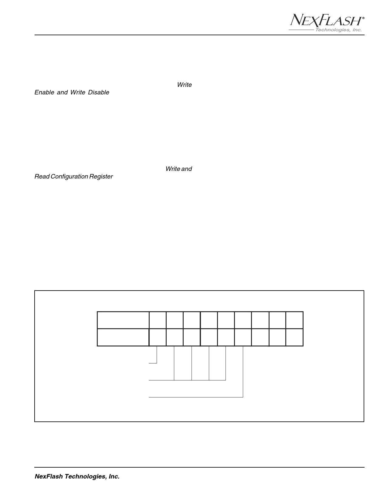
Configuration Register
The Configuration Register stores the current configura-
tion of the reset timing and write protect range (Figure 6).
The configuration register is accessed using the Write and
Read Configuration Register commands. The non-volatile
configuration register will maintain its setting even when
power is removed.
To avoid unnecessary programming of the configuration
register, and to save time during power-up, the
configuration register should be read upon power-up and
compared to the intended setting before sending a Write
Configuration Register command.
The factory default setting for the configuration register is
CF8-CF0 is: 000001001 binary (write protect range = none,
reset time is minimum 1.5µs maximum 5µs). When writing
to the configuration register reserved bits should be 0.
When reading, the settings of reserved bits should be
ignored.
NXS2 Reset Timing (RST)
This bit determines the length of time for the timing
parameter tRESET. With RST reset (0), the timing of tRESET
should be minimum 1.5µs, maximum 5µs. With RST set
(1), the timing of tRESET should be minimum 5µs, maximum
10µs.
Write Protect Range and Direction, WR[3:0], WD
The write protect range and direction bits WR[3:0] and
WD are located at configuration bits CF[7:4] and CF[3]
respectively. The write protect range and direction bits
select how the array is protected. They work in conjunc-
tion with the WP input pin, valid only if WP is inactive (high).
WR[3:0] can select write protection of all sectors, none of
the sectors, or specific sectors grouped in blocks of 64
(~32 KB). The WD bit specifies whether the protected block
range starts from the first sector, address 0 (000H), or
from the last sector (3FFF). Table 2 lists the write protect
sector range for the devices. Once protected, all further
writes to sectors within the range will be ignored. The fac-
tory default setting is with no write protected sectors,
WR=[0,0,0,0] and WD=1.
CF15:9
CF8 CF7 CF6 CF5 CF4 CF3 CF2 CF1 CF0
X = RESERVED
RST WR3 WR2 WR1 WR0 WD X
X
X
RESET TIMING
WRITE PROTECT
RANGE
WRITE PROTECT
DIRECTION
Figure 6. Configuration Register Bit Locations
NexFlash Technologies, Inc.
9
PRELIMINARY NXSF020D-0902
09/05/02 ©
Share Link: 