NX26F640C-3T-R Ver la hoja de datos (PDF) - NexFlash -> Winbond Electronics
Número de pieza
componentes Descripción
Fabricante
NX26F640C-3T-R Datasheet PDF : 23 Pages
| |||
NX26F640C
Pin Descriptions
Pin Assignments
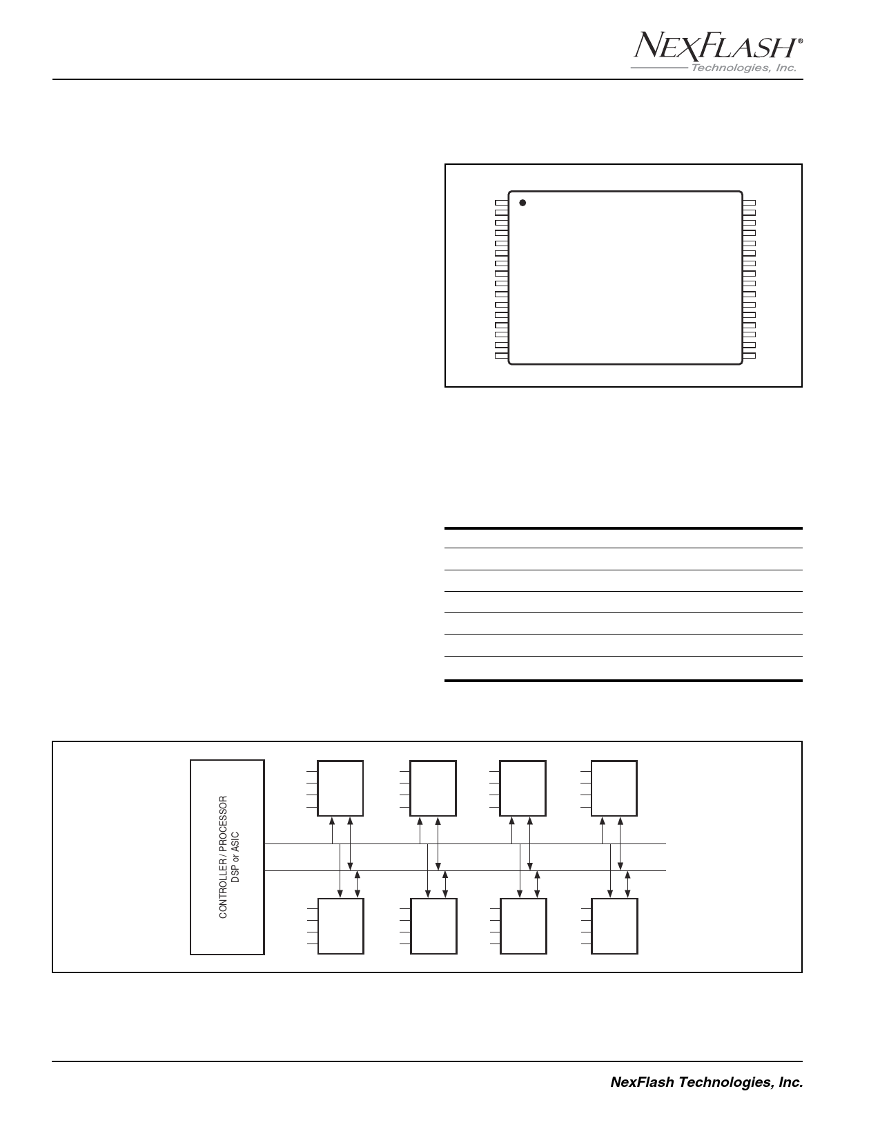
The NX26F640C is available in a 32-Pin TSOP, Type I (T
Package) with an NXS2 Interface (figure 2).
Static Address (A0, A1, A2)
The static address bits allow up to 8 chips to be connected
on the same SCK and SIO pins. The NXS2 protocol selects
the chip to address in the first byte of the command bit
stream by matching the Device Address Field (DA2..0) to
the A2..A0 pins (figure 3).
Serial Data Input/Output (SIO)
The SIO pin transmits data into and out of the device with
the SCK pin. All data transmitted to or from the chip is
clocked relative to the rising edge of SCK.
Serial Clock Input (SCK)
All commands and data written to the SIO pin or read from
the SIO pin are clocked relative to the rising edge of SCK.
When the device is reset, the first low to high transition of
the clock wakes the device up, the second low to high
transition clocks the first command bit to the device on SIO.
When the SIO line switches from an input to an output, the
first transition of the clock switches the direction of the SIO
line to an output.
Chip Enable (CE\)
The Chip Enable pin, when active (low), allows the device
to decode the bit stream on the SCK and SIO pins. When
the Chip Enable pin is not active (high), the device ignores
any bit stream present on the SCK and SIO pins.
Power Supply Pins (Vcc and Gnd)
The NX26F160 supports a single power supply between
2.7V and 3.6V connected to the Vcc and Gnd pins.
A0 1
NC 2
A2 3
NC 4
NC 5
NC 6
VCC 7
GND 8
NC 9
NC 10
NC 11
NC 12
CE
13
SCK 14
A1 15
SIO 16
32
NC
31
NC
30
NC
29
NC
28
NC
27
NC
26
NC
25
NC
24
NC
23
NC
22
NC
21
NC
20
NC
19
NC
18
NC
17
NC
Figure 2. NX26F640C Pin Assignments
NXS2 Interface, 32-Pin TSOP, Type I (T Package)
Table 1. Pin Descriptions
A0, A1, A2
SIO
SCK
CE
VCC
GND
NC
Device Address
Serial Data Input/Output
Serial Clock Input
Chip Enable
Power Supply
Ground
No Connect
0 A0
0 A1 U0
0 A2
0 CE
SCK
1 A0
0 A1 U1
0 A2
0 CE
0 A0
1 A1 U2
0 A2
0 CE
1 A0
1 A1 U3
0 A2
0 CE
SIO
0 A0
0 A1 U4
1 A2
0 CE
1 A0
0 A1 U5
1 A2
0 CE
0 A0
1 A1 U6
1 A2
0 CE
1 A0
1 A1 U7
1 A2
0
CE
Figure 3. NX26F640 Used in a Multi-device Configuration with up to 8-Devices on the same two signals
6
NexFlash Technologies, Inc.
PRELIMINARY NXSF020D-0902
09/05/02 ©
Share Link: 