AT24C01C Ver la hoja de datos (PDF) - Atmel Corporation
NĂșmero de pieza
componentes DescripciĂłn
Fabricante
AT24C01C Datasheet PDF : 23 Pages
| |||
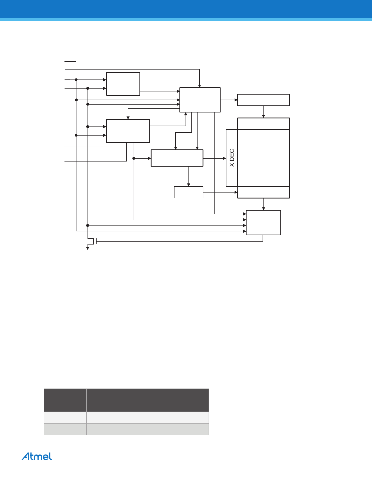
3. Block Diagram
VCC
GND
WP
SCL
SDA
A2
A1
A0
Start
Stop
Logic
LOAD
Device
Address
Comparator
R/W
Serial
Control
Logic
COMP
LOAD INC
EN H.V. Pump/Timing
Data Recovery
Data Word
Addr/counter
EEPROM
DIN
DOUT
Y DEC
Serial MUX
DOUT/ACK
Logic
4. Pin Description
Serial Clock (SCL): The SCL input is used to positive edge clock data into each EEPROM device and negative edge
clock data out of each device.
Serial Data (SDA): The SDA pin is bidirectional for serial data transfer. This pin is open drain driven and may be
wire-ORed with any number of other open drain or open collector devices.
Device/Page Addresses (A2, A1, A0): The A2, A1, and A0 pins are device address inputs that are hard wired for the
AT24C01C/02C. As many as eight 1-Kbit or 2-Kbit devices may be addressed on a single bus system. See Section 7.
âDevice Addressingâ on page 9 for more details.
Write Protect (WP): The AT24C01C/02C have a Write Protect pin that provides hardware data protection. The Write
Protect pin allows normal read/write operations when connected to ground (GND). When the Write Protect pin is
connected to VCC, the write protection feature is enabled and operates as shown below in Table 4-1.
Table 4-1. Write Protect
WP Pin
Status
At VCC
At GND
Part of the Array Protected
Atmel AT24C01C and AT24C02C
Full (2K) Array
Normal Read/Write Operations
Atmel AT24C01C/02C [DATASHEET]
3
8700FâSEEPRâ6/12
Share Link: 