AT17C010 Ver la hoja de datos (PDF) - Atmel Corporation
Número de pieza
componentes Descripción
Fabricante
AT17C010 Datasheet PDF : 13 Pages
| |||
reference the “Programming Specification for Atmel’s FPGA Configuration EEPROMs”
application note.
Programming Mode
The programming mode is entered by bringing SER_EN Low. In this mode the chip can
be programmed by the 2-wire serial bus. The programming is done at VCC supply only.
Programming super voltages are generated inside the chip. See the “Programming
Specification for Atmel’s FPGA Configuration EEPROMs” application note for further
information. The AT17C parts are read/write at 5V nominal. The AT17LV parts are
read/write at 3.3V nominal.
Standby Mode
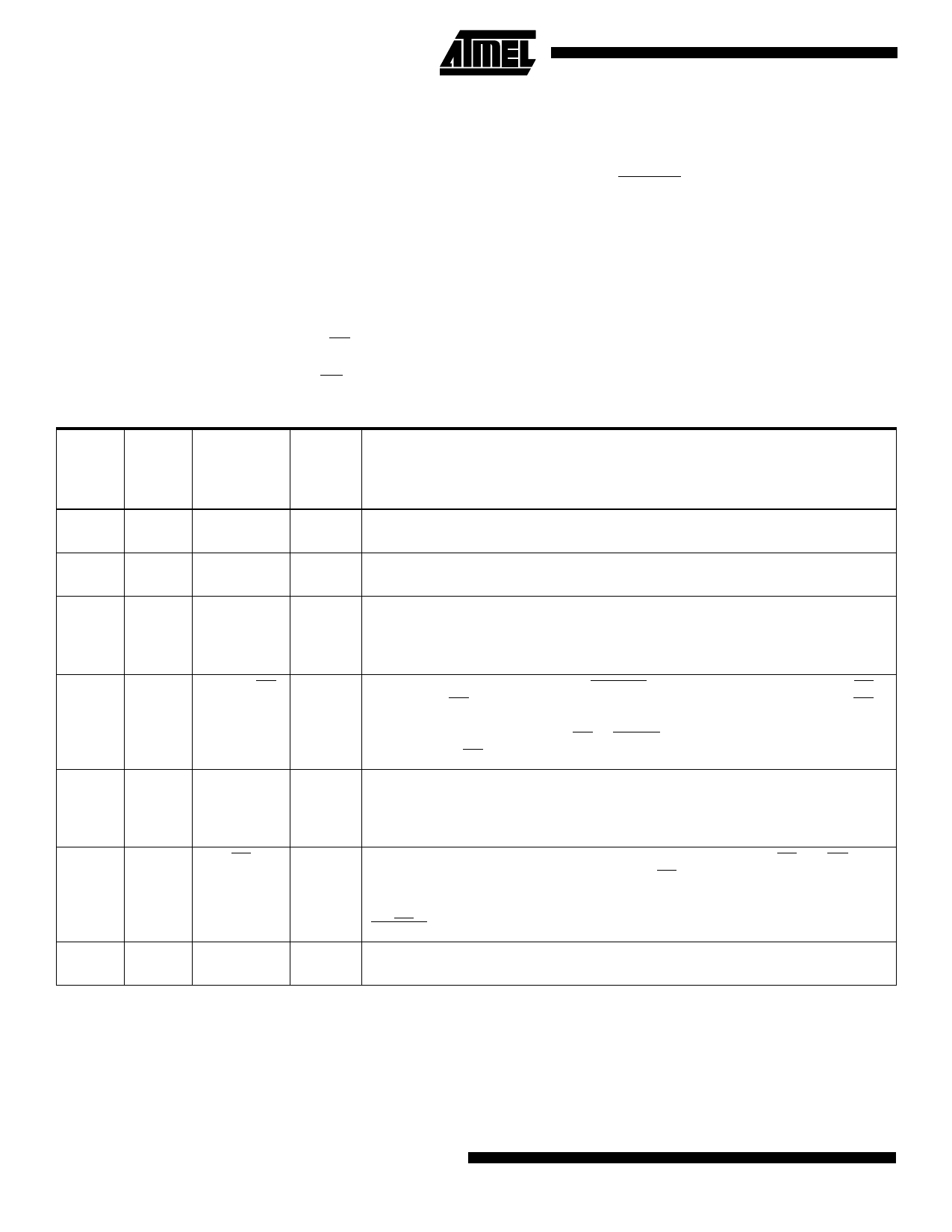
Pin Configurations
The AT17C/LV512/010 Series Configurator enters a low-power standby mode when-
ever CE is asserted High. In this mode, the Configurator consumes less than 0.5 mA of
current at 5V. The output remains in a high impedance state regardless of the state of
the OE input.
8
PDIP/
LAP
Pin
1
20
PLCC
Pin
2
2
4
5
Name
DATA
CLK
WP1
3
6
RESET/OE
7
WP2
4
8
CE
5
10
GND
I/O
Description
I/O
Three-state DATA output for configuration. Open-collector bi-directional pin for
programming.
I
Clock input. Used to increment the internal address and bit counter for reading and
programming.
I
WRITE PROTECT (1). Used to protect portions of memory during programming.
Disabled by default due to internal pull-down resistor. This input pin is not used
during FPGA loading operations. See the “Programming Specification” application
note for more details.
I
RESET/Output Enable input (when SER_EN is High). A Low level on both the CE
and RESET/OE inputs enables the data output driver. A High level on RESET/OE
resets both the address and bit counters. The logic polarity of this input is
programmable as either RESET/OE or RESET/OE. This document describes the
pin as RESET/OE.
I
WRITE PROTECT (2). Used to protect portions of memory during programming.
Disabled by default due to internal pull-down resistor. This input pin is not used
during FPGA loading operations. See the “Programming Specification” application
note for more details.
I
Chip Enable input. Used for device selection. A Low level on both CE and OE
enables the data output driver. A High level on CE disables both the address and bit
counters and forces the device into a low-power standby mode. Note that this pin
will not enable/disable the device in the 2-wire Serial Programming Mode (i.e., when
SER_EN is Low).
Ground pin. A 0.2 µF decoupling capacitor between VCC and GND is
recommended.
4 AT17C512/010/LV512/010
Share Link: 