AT17C010-10PI Ver la hoja de datos (PDF) - Atmel Corporation
Número de pieza
componentes Descripción
Fabricante
AT17C010-10PI Datasheet PDF : 13 Pages
| |||
AT17C512/010/LV512/010
Condition 1
The simplest connection is to have the FPGA CON pin drive both CE and RESET/OE(1)
in parallel. Due to its simplicity, however, this method will fail if the FPGA receives an
external reset condition during the configuration cycle. If a system reset is applied to the
FPGA, it will abort the original configuration and then reset itself for a new configuration,
as intended. Of course, the AT17 Series Configurator does not see the external reset
signal and will not reset its internal address counters and, consequently, will remain out
of sync with the FPGA for the remainder of the configuration cycle.
Note: 1. For this condition, the reset polarity of the EEPROM must be set active High.
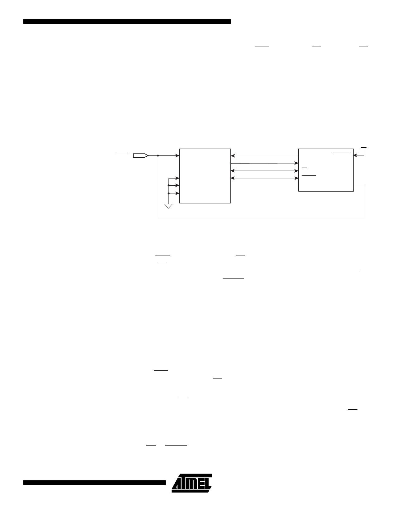
Figure 1. Condition 2 Connection
RESET
AT40K
RESET
M2
M1
M0
D<0>
CCLK
CON
INIT
AT17C512/010
AT17LV512/010
DATA
CLK
CE
RESET/OE
SER_EN
READY
VCC
Condition 2
GND
Notes: 1. Use of the READY pin is optional. The READY pin is not available in the 8-pin
DPDIP/SOIC package.
2. Reset polarity of EEPROM must be set active Low.
The FPGA CON output drives only the CE input of the AT17 Series Configurator, while
the RESET/OE input is driven by the FPGA INIT pin (Figure 1). This connection works
under all normal circumstances, even when the user aborts a configuration before CON
has gone high. A Low level on the RESET/OE(1) input – during FPGA reset – clears the
Configurator’s internal address pointer, so that the reconfiguration starts at the
beginning.
Note: 1. For this condition the reset polarity of the EEPROM must be set active Low.
The AT17 Series Configurator does not require an inverter for either condition since the
RESET polarity is programmable.
Cascading Serial
Configuration
EEPROMs
For multiple FPGAs configured as a daisy-chain, or for future FPGAs requiring larger
configuration memories, cascaded Configurators provide additional memory.
As the last bit from the first Configurator is read, the clock signal to the Configurator
asserts its CEO output Low and disables its DATA line driver. The second Configurator
recognizes the Low level on its CE input and enables its DATA output.
After configuration is complete, the address counters of all cascaded Configurators are
reset if the RESET/OE on each Configurator is driven to its active (default High) level.
If the address counters are not to be reset upon completion, then the RESET/OE input
can be tied to its inactive (default Low) level.
AT17 Series Reset
Polarity
The AT17 Series Configurator allows the user to program the reset polarity as either
RESET/OE or RESET/OE. This feature is supported by industry-standard programmer
algorithms. For more details on programming the EEPROMs reset polarity, please
3
Share Link: 