AT17C010 Ver la hoja de datos (PDF) - Atmel Corporation
Número de pieza
componentes Descripción
Fabricante
AT17C010 Datasheet PDF : 13 Pages
| |||
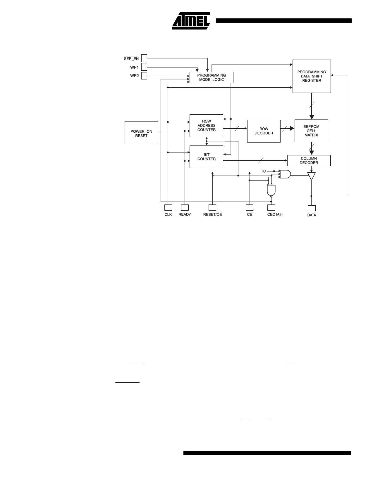
Block Diagram
FPGA Master Serial
Mode Summary
The I/O and logic functions of the FPGA and their associated interconnections are
established by a configuration program. The program is loaded either automatically
upon power-up, or on command, depending on the state of the FPGA mode pins. In
Master Mode, the FPGA automatically loads the configuration program from an external
memory. The AT17 Serial Configuration EEPROM has been designed for compatibility
with the Master Serial Mode.
This document discusses the AT40K FPGA interface. For more details or AT6000
FPGA applications, please reference “AT40K Series Configuration” or “AT6000 Series
Configuration” application notes.
Controlling the High-
density AT17 Series
Serial EEPROMs
During Configuration
Most connections between the FPGA device and the AT17 Serial Configuration
EEPROM are simple and self-explanatory:
The DATA output of the AT17 Series Configurator drives DIN of the FPGA devices.
The master FPGA CCLK output drives the CLK input of the AT17 Series Configurator.
The CEO output of any AT17C/LV512/010 drives the CE input of the next
AT17C/LV512/010 in a cascade chain of EEPROMs.
SER_EN must be connected to VCC (except during ISP).
The READY pin is available as an open-collector indicator of the device’s reset status; it
is driven Low while the device is in its power-on reset cycle and released (tri-stated)
when the cycle is complete. This pin is not available in the 8-pin package.
There are two different ways to use the inputs CE and OE.
2 AT17C512/010/LV512/010
Share Link: 