AS1741 Ver la hoja de datos (PDF) - austriamicrosystems AG
Número de pieza
componentes Descripción
Fabricante
AS1741 Datasheet PDF : 15 Pages
| |||
AS1741, AS1742, AS1743
Data Sheet
austriamicrosystems
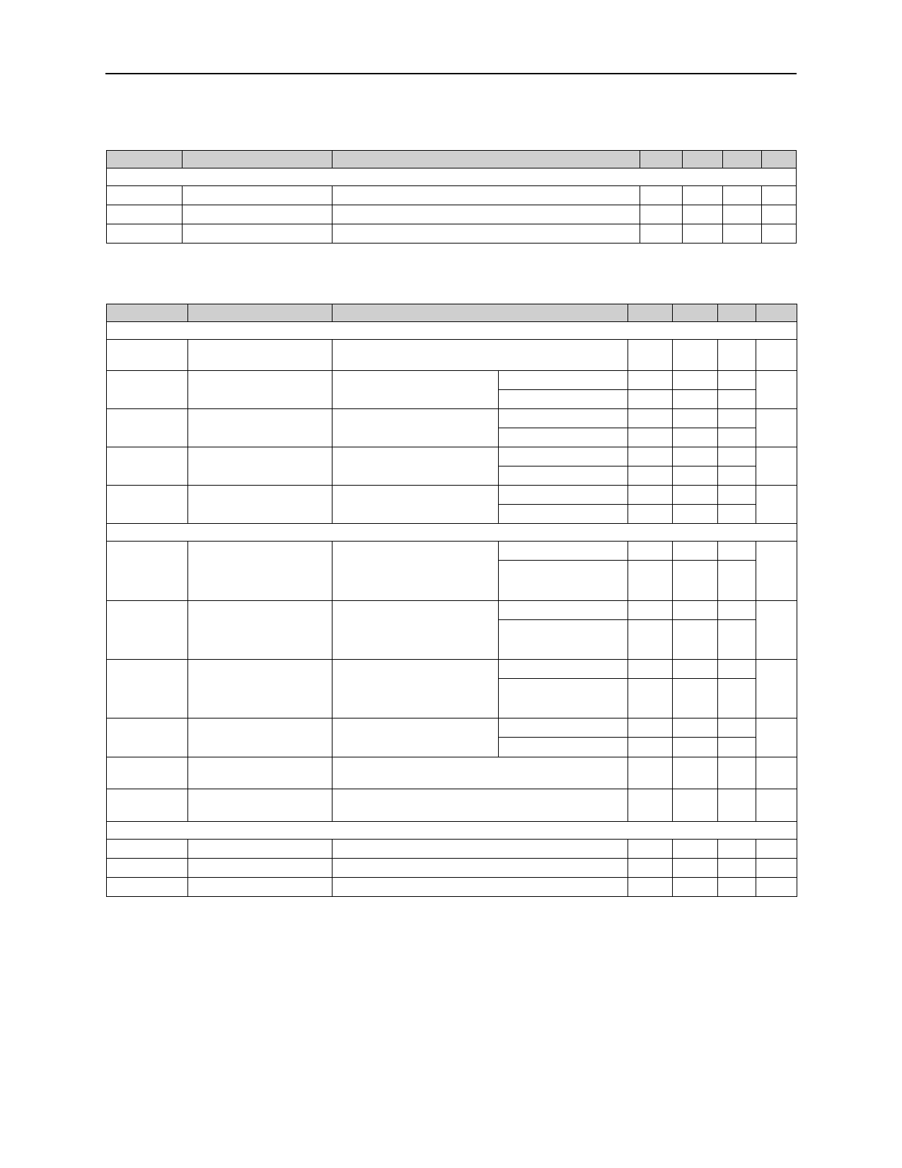
Table 4. +3V Supply Electrical Characteristics (Continued)
Symbol
Logic Input
Parameter
Conditions
VIH
Input Logic High
VIL
Input Logic Low
IIN
Input Leakage Current
VINx = 0 or V+
Min Typ Max Unit
1.4
V
0.5 V
-1000 0.1 1000 nA
V+ = +1.8V, VIH = +1.0V, VIL = 0.4V, TAMB = TMIN to TMAX (unless otherwise specified). Typ values @ TAMB = +25ºC.
Table 5. +1.8V Supply Electrical Characteristics
Symbol
Parameter
Conditions
Min
Analog Switch
VCOMx,
VNOx, VNCx
Analog Signal Range
0
RON
ON-Resistance
ICOMx = 10mA,
VNOx or VNCx = 0.9V
TAMB = +25ºC
TAMB = TMIN to TMAX
INOx(OFF),
INCx(OFF)
NOx or NCx Off-
Leakage Current
VCOMx = 0.3 or 1.5V, VNOx
TAMB = +25ºC
-1
or VNCx = 1.5 or 0.3V TAMB = TMIN to TMAX -5
ICOMx(OFF)
COMx Off-Leakage VCOMx = 0.3 or 1.5V, VNOx
TAMB = +25ºC
-1
Current
or VNCx = 1.5 or 0.3V TAMB = TMIN to TMAX -5
ICOMx(ON)
COMx On-Leakage
VCOMx = 0.3 or 1.5V,
TAMB = +25ºC
-2
Current
VNOx or VNCx = 0.3 or 1.5V TAMB = TMIN to TMAX -10
Switch Dynamic Characteristics
VNOx or VNCx = 1.5V,
TAMB = +25ºC
tON
Turn On Time 3
RLOAD = 50Ω,
CLOAD = 35pF,
TAMB = TMIN to TMAX
Figures 12, 13
tOFF
Turn Off Time 3
VNOx or VNCx = 1.5V,
RLOAD = 50Ω,
CLOAD = 35pF,
Figures 12, 13
TAMB = +25ºC
TAMB = TMIN to TMAX
tBBM
Break-Before-Make 3
VNOx or VNCx = 1.5V,
RLOAD = 50Ω,
CLOAD = 35p,
Figure 14, (AS1743)
TAMB = +25ºC
TAMB = TMIN to TMAX 1
Q
Charge Injection
VGEN = 1.8V, RGEN = 0,
CLOAD = 1.0nF, Figure 15
8-pin MSOP
8-pin SOT23
VISO
Off-Isolation 4
f = 1MHz, VCOMx = 1VRMS,
RLOAD = 50Ω, CLOAD = 5pF, Figure 17
Logic Input
VIH
Crosstalk 5
Input Logic High
f = 1MHz, VCOMx = 1VRMS,
RLOAD = 50Ω, CLOAD = 5pF, Figure 17
1
VIL
Input Logic Low
IIN
Input Leakage Current
VINx = 0 or V+
-1000
Typ
0.9
21
12
8
6
2.5
-50
-100
0.1
Max Unit
V+ V
2.5
Ω
3
1
nA
5
1
nA
5
2
nA
10
30
ns
35
20
ns
25
ns
pC
dB
dB
V
0.4 V
1000 nA
1. ∆RON = RON(MAX) - RON(MIN).
2. Flatness is defined as the difference between the maximum and the minimum value of ON-resistance as measured
over the specified analog signal ranges.
3. Guaranteed by design.
4. Off-Isolation = 20log10(VCOMx/VNOx), VCOMx = output, VNOx = input to off switch.
5. Between two switches.
www.austriamicrosystems.com
Revision 1.76
4 - 15
Share Link: 