AS1507 Ver la hoja de datos (PDF) - austriamicrosystems AG
Número de pieza
componentes Descripción
Fabricante
AS1507
austriamicrosystems AG

AS1507 Datasheet PDF : 17 Pages
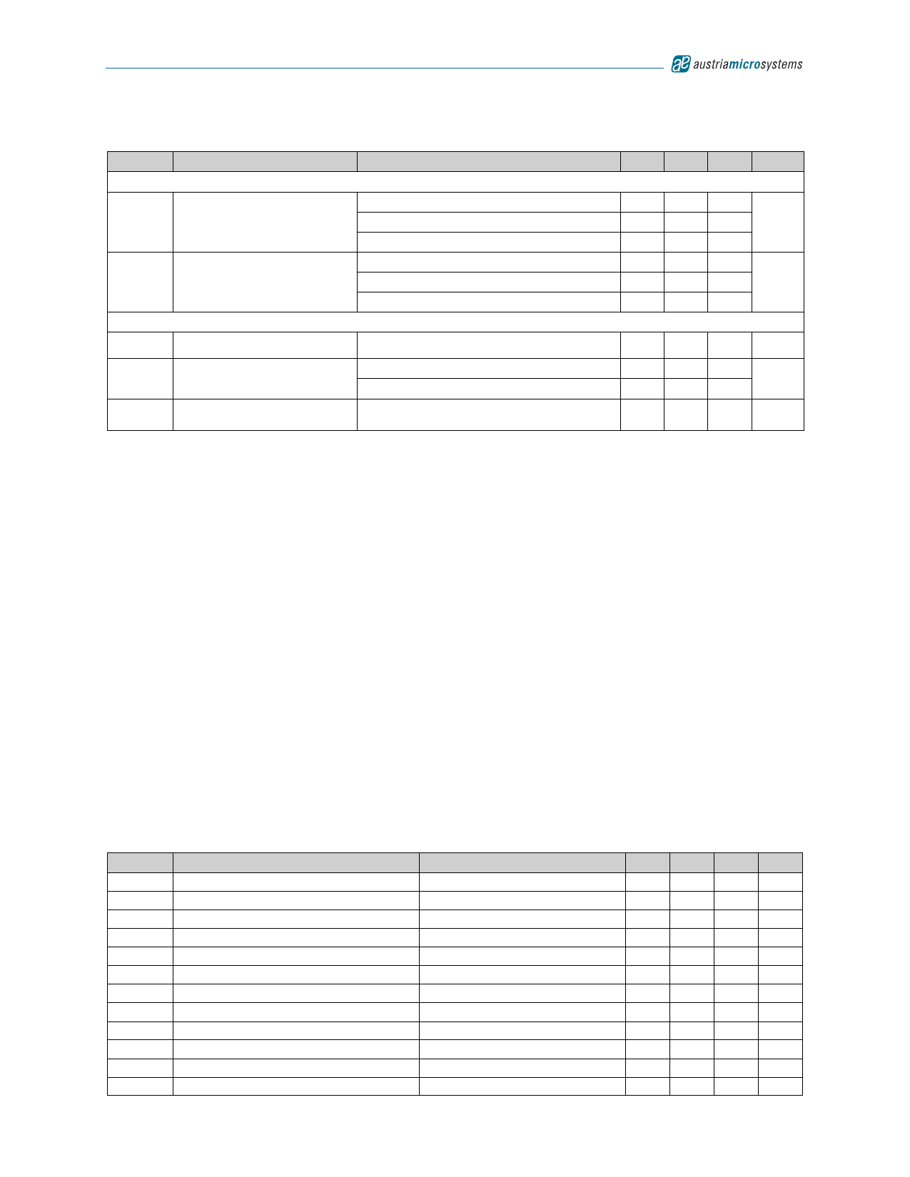
| |||
AS1507
Data Sheet - Electrical Characteristics
Table 4. Electrical Characteristics (Continued)
Symbol
Parameter
Dynamic Characteristics
Wiper -3dB Bandwidth 6
tS
Wiper Settling Time7
Non-Volatile Memory Reliability
Data Retention 8
Endurance 8
tBUSY
Write Non-Volatile Register
Busy Time
Condition
AS1507-10
AS1507-50
AS1507-100
AS1507-10
AS1507-50
AS1507-100
TAMB = +85ºC
TAMB = +25ºC
TAMB = +85ºC
Min Typ Max Unit
1200
220
kHz
120
1100
1600
ns
2200
150
Years
10M
Write
1M
Cycles
20 ms
1. The programming current operates only during power-up and non-volatile memory writes.
2. DNL and INL are measured with the potentiometer configured as a voltage-divider with HIGH = VDD and LOW =
GND. The wiper terminal is unloaded and measured with a high-input-impedance voltmeter.
3. DNL and INL are measured with the potentiometer configured as a variable resistor. HIGH is unconnected and
LOW = GND. For the 5V condition, the wiper terminal is driven with a source current of 400µA @ 10kΩ, 80µA @
50kΩ, 40µA @ 100kΩ. In 3V conditions, the wiper terminal is driven with a source current of 200µA @ 10kΩ,
40µA @ 50kΩ, 20µA @ 100kΩ.
4. The wiper resistance is measured using the source currents given in Note 3. The number is the worst case
resistance over TAP positions.
5. The device draws higher supply current when the digital inputs are driven with voltages between (VDD - 0.5V)
and (GND + 0.5V).
6. Wiper at midscale with a 10pF load (DC measurement) VDD = 5V, LOW = GND. An AC source (5V peak to peak
sinus signal) is applied to HIGH and the WIPER output is measured. A 3dB bandwidth occurs when the AC
WIPER/HIGH value is 3dB lower than the DC WIPER/HIGH value.
7. Wiper-settling time is the worst-case 0 to 50% rise-time measured between successive wiper positions. HIGH =
VDD, LOW = GND; WIPER is unloaded and measured with a 10pF load.
8. This parameter is not tested but ensured by characterization.
Timing Characteristics
VDD = +2.7 to +5.5V, HIGH = VDD, LOW = GND, TAMB = -40 to +85ºC. Typ values are at VDD = +5.0V, TAMB = +25ºC
(unless otherwise specified). See Figure 20 on page 9. Digital timing data is guaranteed by design and characteriza-
tion, and is not production tested.
Table 5. Timing Characteristics
Symbol
fSCLK
tCP
tCH
tCL80
tCSS
tCSH
tDS
tDH
tCS0
tCS1
tCSW
tBUSY
Parameter
SCLK Frequency
SCLK Clock Period
SCLK Pulse-Width High
SCLK Pulse-Width Low
CSN-Fall to SCLK Rise Setup
SCLK-Rise to CSN-Rise Hold
SDIO to SCLK Setup
SDIO Hold after SCLK
SCLK-Rise to CSN-Fall Delay
CSN-Rise to SCLK-Rise Hold
CSN Pulse-Width High
Write Non-Volatile Register Busy Time
Condition
Min Typ Max Unit
5 MHz
200
ns
40
ns
40
ns
40
ns
40
ns
10
ns
0
ns
40
ns
40
ns
200
ns
20 ms
www.austriamicrosystems.com
Revision 1.00
5 - 17
Share Link: