AS1501-Z Ver la hoja de datos (PDF) - austriamicrosystems AG
Número de pieza
componentes Descripción
Fabricante
AS1501-Z Datasheet PDF : 8 Pages
| |||
Data Sheet AS1500/1/2/3
AS150x – SPECIFICATIONS
(VDD = 3V±10% or 5V±10%, VA = VDD, VB = 0V,
–40°C≤TA≤+125°C unless otherwise noted.)
ELECTRICAL CHARACTERISTICS–ALL
VERSIONS
Parameter
Sym-
bol
Conditions
Min
Typ
21
Max
Unit
SWITCHING CHARACTERISTICS 22, 23
Input Clock
Pulsewidth
tCH,
tCL
Clock Level
High or Low
50
ns
Data Setup Time
tDS
5
ns
Data Hold Time
tDH
5
ns
CSN Setup Time
tCSS
10
ns
CSN High
Pulsewidth
tCSW
10
ns
CK Fall to CSN Rise
Hold Time
tCSH
0
ns
CSN Rise to Clock
Rise Setup
tCS1
10
ns
Table 5: Switching Characteristics
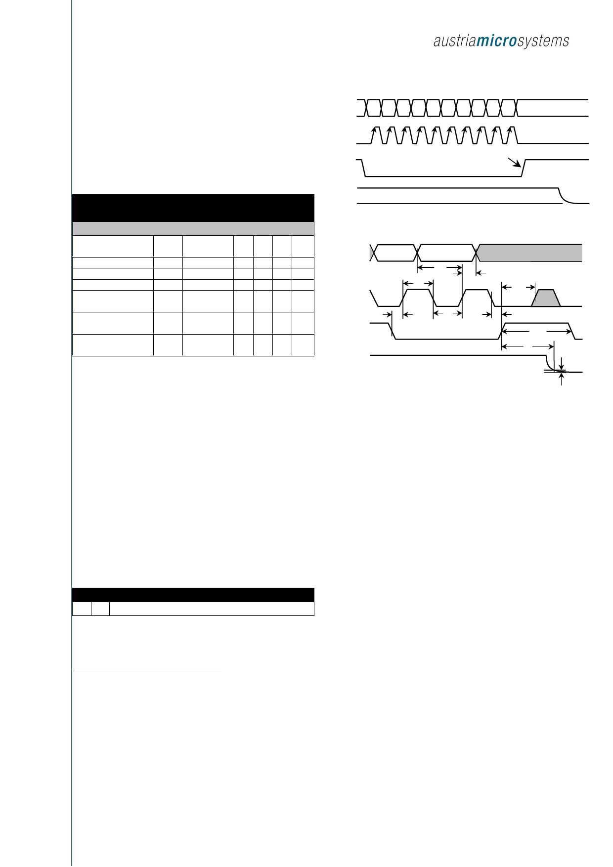
Detailed Description
Serial-Programming
Programming of the AS150x is done via the 3 wire serial
interface. The three input signals are serial data input
(SDI), clock(CK) and chip select (CS). A programming
sequence consists of 10-bit, where the last eight bit
contain the code word for the resistor value. The first two
bits A1 and A0 have to be low(see Table ). The data is
shifted into the internal 10 Bit register with the rising edge
of the CK signal. With the rising edge of the CSN signal
the data becomes valid and the resistance is updated (see
figure 2). A detailed block diagram is shown in figure 3.
A1 A0 D7 D6 D5 D4 D3 D2 D1 D0
0 0 MSB
Data
LSB
Table 6: Serial data format (16 bits)
1
SD
0
CK 1
0
1
CS
0
V
VD
OUT
0V
A1 A0 D7 D6 D5 D4 D3 D2 D1 D0
DAC Register
Figure 2: Timing Diagram
SDI 1
0
1
CK
0
1
CSN
0
V
O
VDD
UT
0V
AX or
tC
tCS
AX or
tD
tD
tCL
tCS
tCS
tCS
tS
±1% Error
Figure 3: Detailed Timing Diagram
±1%
Rheostat Operation
The digital potentiometer family AS150x offers nominal
resistor values of 10kΩ, 20 kΩ, 50kΩ and 100kΩ. The
resistor has 256 contact points where the wiper can access
the resistor. The 8-bit code word determines the position
of the wiper and is decoded through an internal logic. The
lowest code 00h is related to the terminal B. The
resistance is then only determined by the wiper resistance
(100Ω). The resistance for the next code 01h is the
nominal resistor RAB (10kΩ, 20 kΩ, 50kΩ or 100kΩ)
divided through 256 plus the wiper resistor. In case of
AS1501 (10kΩ) the total resistance is 39Ω+100Ω=139Ω.
Accordingly the resistor for code 02h is 78Ω+100Ω=178Ω.
The last code 255h does not connect to terminal A directly
(see Figure 5). So the maximum value is 10000Ω - 39Ω
+100Ω = 10061Ω. The general formula for the calculation
of the resistance RWB is:
21 Typicals represent average readings at 25°C and VDD=5V.
22 Guaranteed by design and not subject to production test.
Resistor-terminal capacitance tests are measured with 2.5V
bias on the measured terminal. The remaining resistor
terminals are left open circuit.
23 See timing diagram for location of measured values. All input
control voltages are specified with tR = tF = 1ns (10% to 90% of
VDD) and timed from a voltage level of 1.6V. Switching
characteristics are measured using VDD=3V or 5V. To avoid
false clocking, a minimum input logic slew rate of 1V/µs should
be maintained.
Revision 1.0, Oct 2004
RWB (Dx)= (Dx)/256⋅RAB + RW
where RAB is the nominal resistance between terminal A
and B, RW is the wiper resistance and DX is the 8-Bit Code
word. In Table 7 the resistor values between the wiper and
terminal B for AS1501 are given for specific codes DX. In
the zero-scale condition the wiper resistance of 100Ω
remains present.
Page 5 of 8
Share Link: 