AS1161 Ver la hoja de datos (PDF) - austriamicrosystems AG
Número de pieza
componentes Descripción
Fabricante
AS1161
austriamicrosystems AG

AS1161 Datasheet PDF : 29 Pages
| |||
AS1160/AS1161
Datasheet - Electrical Characteristics
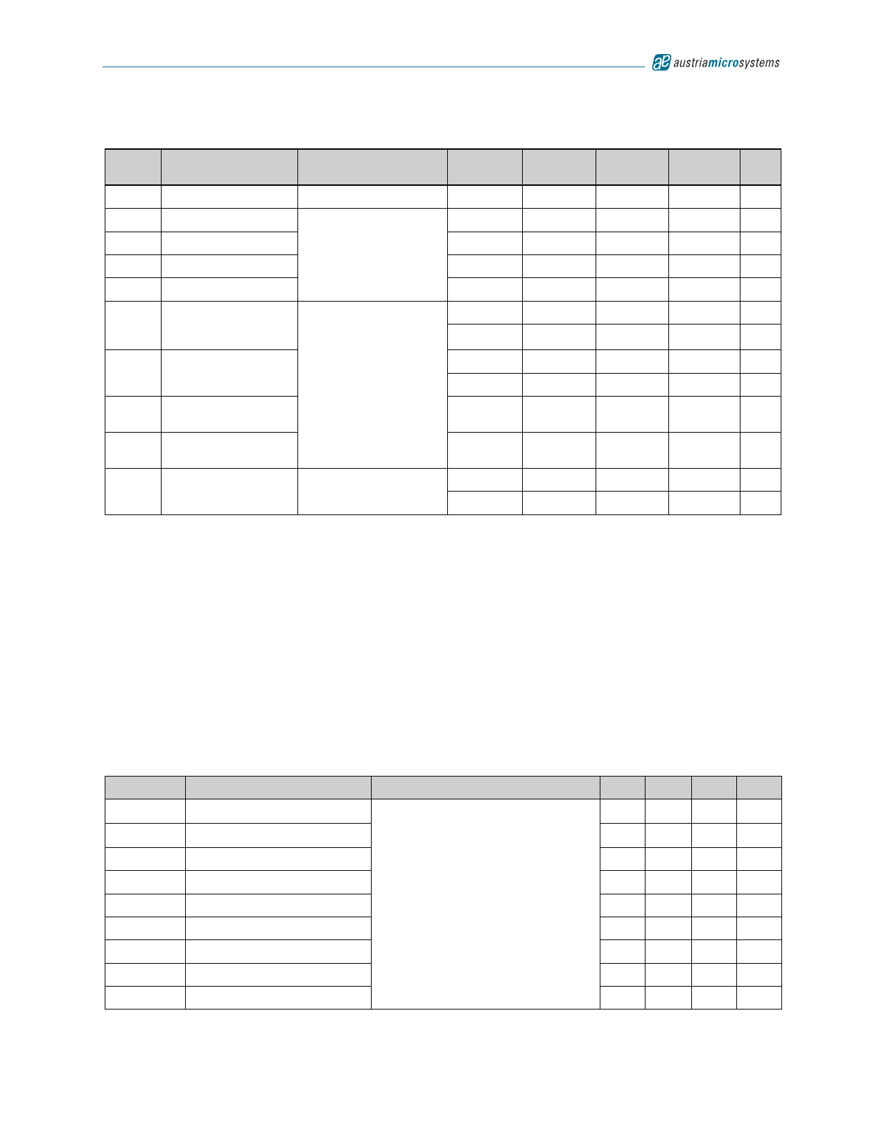
Table 9. Deserializer Switching Characteristics1
Symbol
Parameter
Conditions
Pin/
Frequency
Min
tRDC
RCLK Duty Cycle
45
tHZR High to Tri-State Delay
ROUTx
3
tLZR Low to Tri-State Delay
ROUTx
3
Figure 29 on page 16
tZHR Tri-State to High Delay
ROUTx
4
tZLR Tri-State to Low Delay
ROUTx
4
Deserializer PLL Lock
tDSR12 Time from PWDNN
(with SYNCPAT)
20MHz
66MHz
tDSR22
Deserializer PLL Lock
Time from SYNCPAT
tZHLK
Tri-State to High Delay
(Powerup)
Figure 30 on page 17,
Figure 31 on page 17
20MHz
66MHz
LOCKN
tRCLKL1
RCLK low time before
LOCK achieved
RCLK
tRNM3
Deserializer Noise
Margin
Figure 33 on page 18
20MHz
66MHz
0.8
200
Typ
50
6
6
6
6
5.2
1.8
5.1
1.9
4
32xtRFCP
1
300
Max Unit
55
ns
ns
ns
ns
ns
7.5
µs
3
µs
7.5
µs
3
µs
12
ns
ns
ns
ps
1. Guaranteed by simulation and characterization.
2. For the purpose of specifying deserializer PLL performance, tDSR1 and tDSR2 are specified with the REFCLK
running and stable, and with specific conditions for the incoming data stream synchronization patterns (SYNC-
PATs). The derserializer should be initialized using either tDSR1 or tDSR2.
tDSR1 is the time required for the deserializer to indicate lock upon power-up or when leaving the power-down
mode. SYNCPATs should be sent to the device before initiating either condition.
tDSR2 is the time required to indicate lock for the powered-up and enabled deserializer when the input (RI+ and
RI-) conditions change from not receiving data to receiving SYNCPATs.
3. tRNM is a measure of how much phase noise (jitter) the deserializer can tolerate in the incoming data stream
before bit errors occur. The deserializer noise margin is guaranteed by design using statistical analysis.
Scan Circuitry Timing Requirements
Table 10. Scan Circuitry Timing Requirements
Symbol
Parameter
fTCK
TCK Clock Frequency
tTCK
TCK Clock Period
tS
TCK to TDI, TMS Setup Time
tH
TCK to TDI, TMS Hold Time
tWH, tWL TCK Pulse Width, High or Low
tWR
TRSTN Pulse Width, Low
tREC TRSTN-to-TCK Recovery Time
tD
TCK to TDO Delay
tZ
TCK to TDO High Z Delay
Conditions
Figure 15 on page 12
Min Typ Max Unit
25
MHz
40
ns
2.0
ns
3.0
ns
10.0
ns
2.5
ns
2.0
ns
10 ns
10 ns
Note: All limits are guaranteed. The parameters with min and max values are guaranteed with production tests or
SQC (Statistical Quality Control) methods.
www.austriamicrosystems.com/Interfaces-LVDS/AS1160_61
Revision 1.01
9 - 29
Share Link: