AS1115 Ver la hoja de datos (PDF) - austriamicrosystems AG
Nأ؛mero de pieza
componentes Descripciأ³n
Fabricante
AS1115 Datasheet PDF : 24 Pages
| |||
AS1115
Datasheet - Absolute Maximum Ratings
5 Absolute Maximum Ratings
Stresses beyond those listed in Table 2 may cause permanent damage to the device. These are stress ratings only,
and functional operation of the device at these or any other conditions beyond those indicated in Section 6 Electrical
Characteristics on page 4 is not implied. Exposure to absolute maximum rating conditions for extended periods may
affect device reliability.
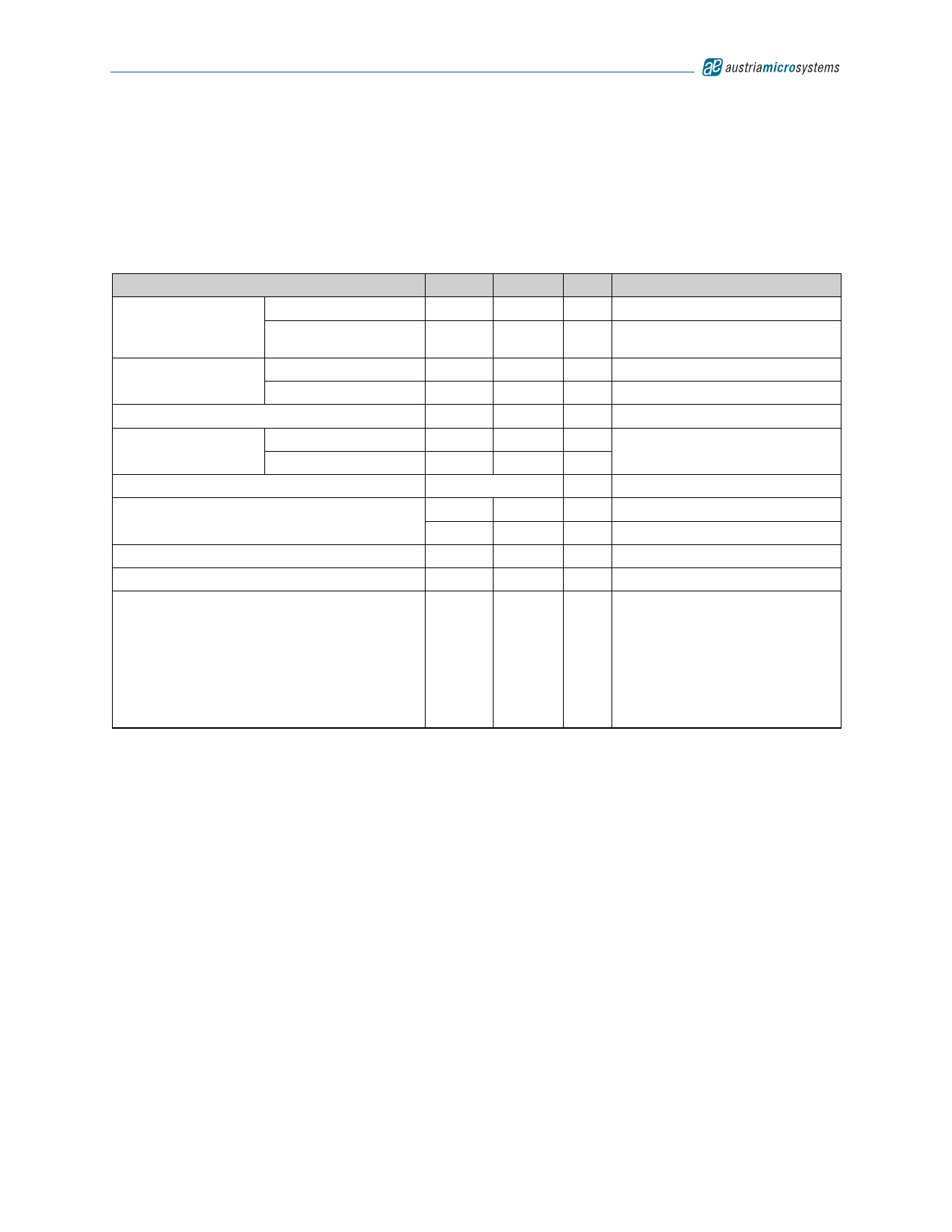
Table 2. Absolute Maximum Ratings
Parameter
Min
Max Units
Notes
Input Voltage Range
VDD to GND
All other pins to GND
-0.3
7
V
-0.3
7 or
VDD + 0.3
V
Current
DIG0:DIG7 Sink Current
SEGA:SEGG, SEGDP
500
mA
100
mA
Humidity
5
85
%
Non-condensing
Electrostatic Discharge
Digital outputs
All other pins
Latch-Up Immunity
Thermal Resistance خکJA
Ambient Temperature
1000
1000
آ±100
88
30.5
-40
+85
V
V
mA
آ؛C/W
آ؛C/W
آ؛C
Norm: MIL 833 E method 3015
EIA/JESD78
on PCB, QSOP-24 package
on PCB, TQFN(4x4)-24 package
Storage Temperature
-55
150
آ؛C
Package Body Temperature
+260
The reflow peak soldering
temperature (body temperature)
specified is in accordance with IPC/
JEDEC J-STD-020D “Moisture/
آ؛C Reflow Sensitivity Classification for
Non-Hermetic Solid State Surface
Mount Devicesâ€.
The lead finish for Pb-free leaded
packages is matte tin (100% Sn).
www.austriamicrosystems.com
Revision 1.03
3 - 24
Share Link: 