AS1108 Ver la hoja de datos (PDF) - austriamicrosystems AG
Número de pieza
componentes Descripción
Fabricante
AS1108 Datasheet PDF : 19 Pages
| |||
AS1108
Data Sheet
austriamicrosystems
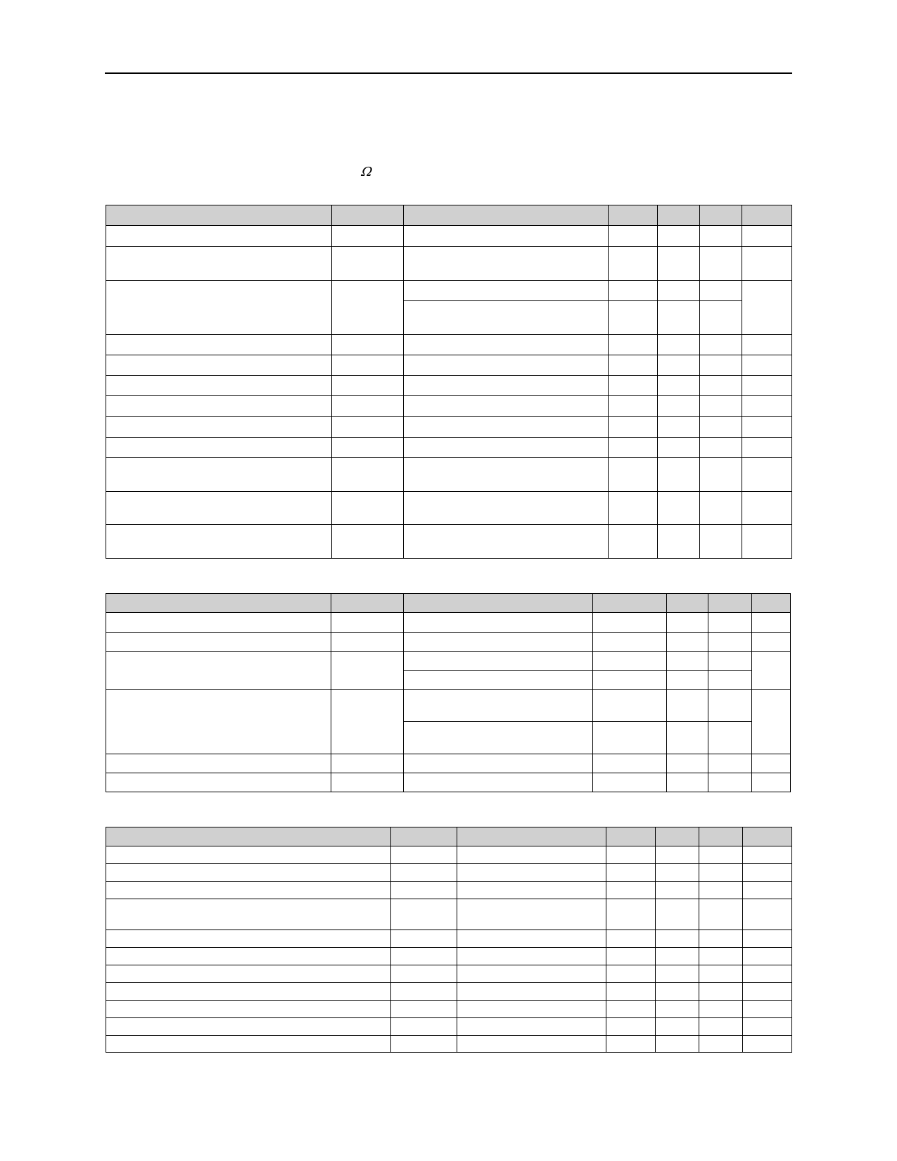
5 Electrical Characteristics
Conditions: VDD = 2.7 to 5.5V, RSET = 9.53kΩ±1%, TAMB = TMIN to TMAX (unless otherwise specified).
Table 2. Electrical Characteristics
Parameter
Symbol
Conditions
Min Typ Max
Operating Supply Voltage
VDD
2.7 5.0 5.5
Shutdown Supply Current
IDDSD
All digital inputs at VDD or GND,
TAMB = +25ºC
10
Operating Supply Current
RSET = open circuit.
IDD
All segments and decimal point
on; ISEG = -40mA.
1
330
Display Scan Rate
fOSC
4 digits scanned
1000 1600 2600
Digit Drive Sink Current
IDIGIT
VOUT = 0.65V
320
Segment Drive Source Current
ISEG
VDD = 5.0V, VOUT = (VDD -1V) -30 -40 -45
Segment Drive Current Matching
ΔISEG
3.0
Digit Drive Source Current
IDIGIT
Digit off, VDIGIT = (VDD - 0.3V)
-2
Segment Drive Sink Current
ISEG
Segment off, VSEG = 0.3V
5
Slow Segment Blink Period (ON
phase, Internal Oscillator)
tSLOWBLINK
0.64 1 1.65
Fast Segment Blink Period
(ON phase, Internal Oscillator)
tFASTBLINK
0.32 0.5 0.83
Fast or Slow Segment Blink Duty
Cycle (Guaranteed by design)
49.9 50 50.1
Unit
V
µA
mA
Hz
mA
mA
%
mA
mA
s
s
%
Table 3. Logic Inputs/Outputs Characteristics
Parameter
Input Current DIN, CLK, LOAD/CSN
Logic High Input Voltage
Symbol
IIH, IIL
VIH
Logic Low Input Voltage
VIL
Output High Voltage
VOH
Output Low Voltage
VOL
Hysteresis Voltage
ΔVI
Conditions
VIN = 0V or VDD
VDD = 5.0V ± 10%
VDD = 3.0V ± 10%
DOUT, ISOURCE = -1mA,
VDD = 5.0V ± 10%
DOUT, ISOURCE = -1mA,
VDD = 3.0V ± 10%
DOUT, ISINK = 1.6mA
DIN, CLK, LOAD/CSN
Min
Typ Max Unit
-1
1 µA
0.7 x VDD
V
0.8
V
0.6
VDD - 1
V
VDD - 0.5
0.4 V
1
V
Table 4. Timing Characteristics
Parameter
CLK Clock Period
CLK Pulse Width High
CLK Pulse Width Low
CSMFall-to-CLK Rise Setup Time
(AS1108 SPI-programmed)
CLK Rise-to -LOAD/CSN Rise Hold Time
DIN Setup Time
DIN Hold Time
Output Data Propagation Delay
LOAD Rising Edge-to-Next Clock Rising Edge
Minimum LOAD/CSN Pulse High
Data-to-Segment Delay
Symbol
tCP
tCH
tCL
tCSS
tCSH
tDS
tDH
tDO
tLDCK
tCSW
tDSPD
Conditions
CLOAD = 50pF
Note: See Figure 9 on page 6 for additional timing information.
Min Typ Max Unit
100
ns
50
ns
50
ns
25
ns
0
ns
25
ns
0
ns
25 ns
50
ns
50
ns
2.25 ms
www.austriamicrosystems.com
Revision 2.1
3 - 19
Share Link: 