AS1108 Ver la hoja de datos (PDF) - austriamicrosystems AG
Número de pieza
componentes Descripción
Fabricante
AS1108 Datasheet PDF : 19 Pages
| |||
AS1108
Data Sheet
austriamicrosystems
Digit- and Control-Registers
Feature Register (0xXE)
The Feature Register is used for switching the device into external clock mode, applying an external reset, selecting
code-B or HEX decoding, enabling or disabling blinking, enabling or disabling the SPI-compatible interface, setting the
blinking rate, and resetting the blink timing.
Note: At power-up the Feature Register is initialized to 0.
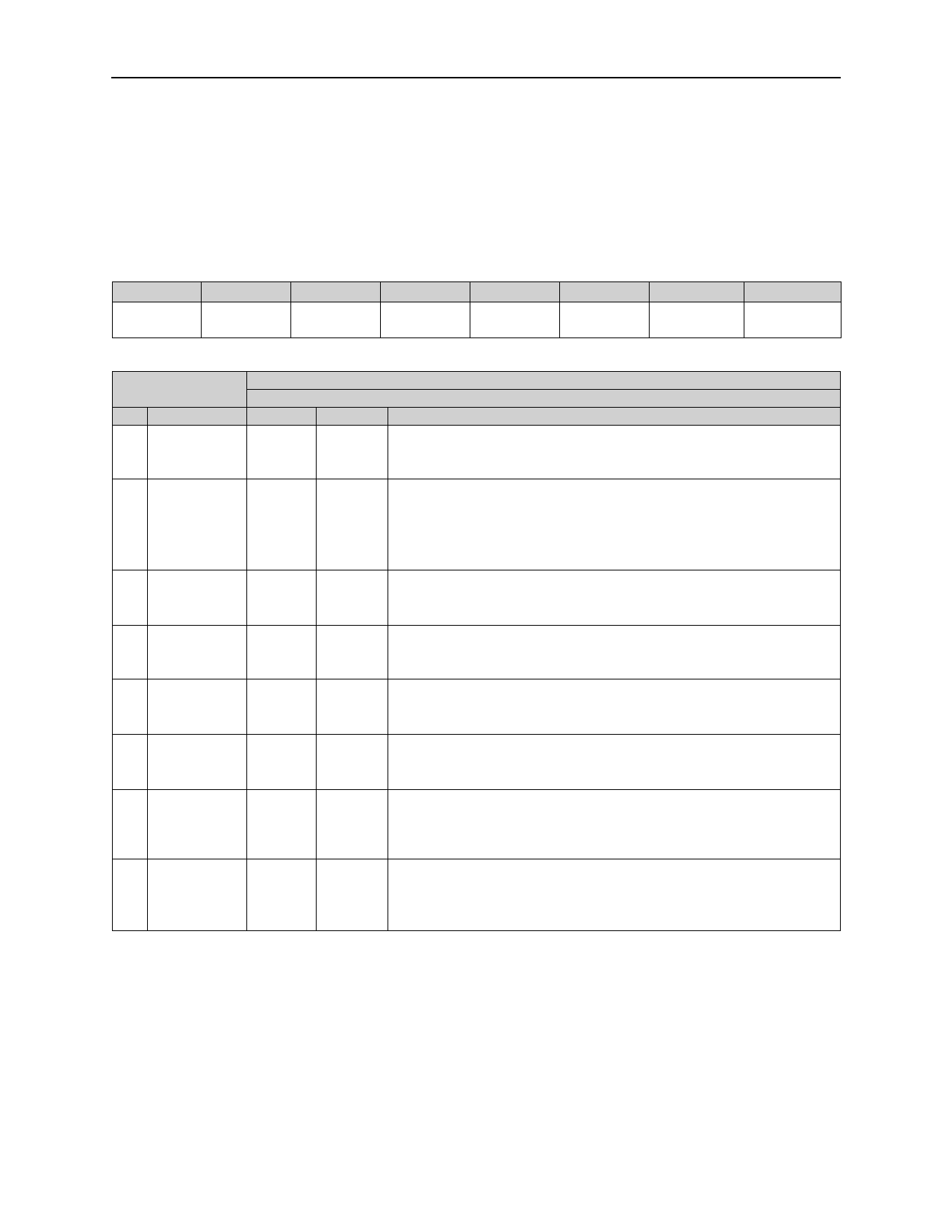
Table 16. Feature Register Summary
D7
blink_
start
D6
sync
D5
blink_
freq_sel
D4
blink_en
D3
spi_en
D2
decode_sel
D1
reg_res
D0
clk_en
Table 17. Feature Register Bit Descriptions (Address (HEX) = 0xXE))
Addr: 0xXE
Feature Register
Enables and disables various device features.
Bit Bit Name Default Access
Bit Description
External clock select.
D0
clk_en
0
R/W 0 = Internal oscillator is used for system clock.
1 = Pin CLK of the serial interface operates as system clock input.
Resets all control registers except the Feature Register.
0 = Reset Disabled. Normal operation.
D1 reg_res
0
R/W 1 = All control registers are reset to default state (except the Feature
Register) identically after power-up.
Note: The Digit Registers maintain their data.
Selects display decoding.
D2 decode_sel
0
R/W 0 = Enable Code-B decoding (see Table 9 on page 8).
1 = Enable HEX decoding (see Table 10 on page 9).
Enables the SPI-compatible interface.
D3
spi_en
0
R/W 0 = Disable SPI-compatible interface.
1 = Enable the SPI-compatible interface.
Enables blinking.
D4 blink_en
0
R/W 0 = Disable blinking.
1 = Enable blinking.
Sets blink with low frequency (with the internal oscillator enabled):
D5 blink_freq_sel
0
R/W 0 = Blink period typically is 1 second (0.5s on, 0.5s off).
1 = Blink period is 2 seconds (1s on, 1s off).
Synchronizes blinking on the rising edge of pin LOAD/CSN. The
D6
sync
0
R/W
multiplex and blink timing counter is cleared on the rising edge of pin
LOAD/CSN. By setting this bit in multiple AS1108 devices, the blink
timing can be synchronized across all the devices.
Start Blinking with display enabled phase. When bit D4 (blink_en) is set,
D7 blink_start
0
bit D7 determines how blinking starts.
R/W 0 = Blinking starts with the display turned off.
1 = Blinking starts with the display turned on.
No-Op Register (0xX0)
The No-Op Register is used when multiple AS1108 devices are cascaded in order to support displays with more than 4
digits. The cascading must be done in such a way that all DOUT pins are connected to DIN of the next AS1108 (see
Figure 11 on page 14). The LOAD/CSN and CLK signals are connected to all devices.
For example, if five devices are cascaded, in order to perform a write operation to the fifth device, the write-command
must be followed by four no-operation commands. When the LOAD/CSN signal goes high, all shift registers are
latched. The first four devices will receive no-operation commands and only the fifth device will receive the intended
operation command, and subsequently update its register.
www.austriamicrosystems.com
Revision 2.1
11 - 19
Share Link: 