AS1332 Ver la hoja de datos (PDF) - austriamicrosystems AG
Número de pieza
componentes Descripción
Fabricante
AS1332 Datasheet PDF : 20 Pages
| |||
AS1332
Datasheet - Absolute Maximum Ratings
5 Absolute Maximum Ratings
Stresses beyond those listed in Table 2 may cause permanent damage to the device. These are stress ratings only,
and functional operation of the device at these or any other conditions beyond those indicated in Electrical
Characteristics on page 4 is not implied. Exposure to absolute maximum rating conditions for extended periods may
affect device reliability.
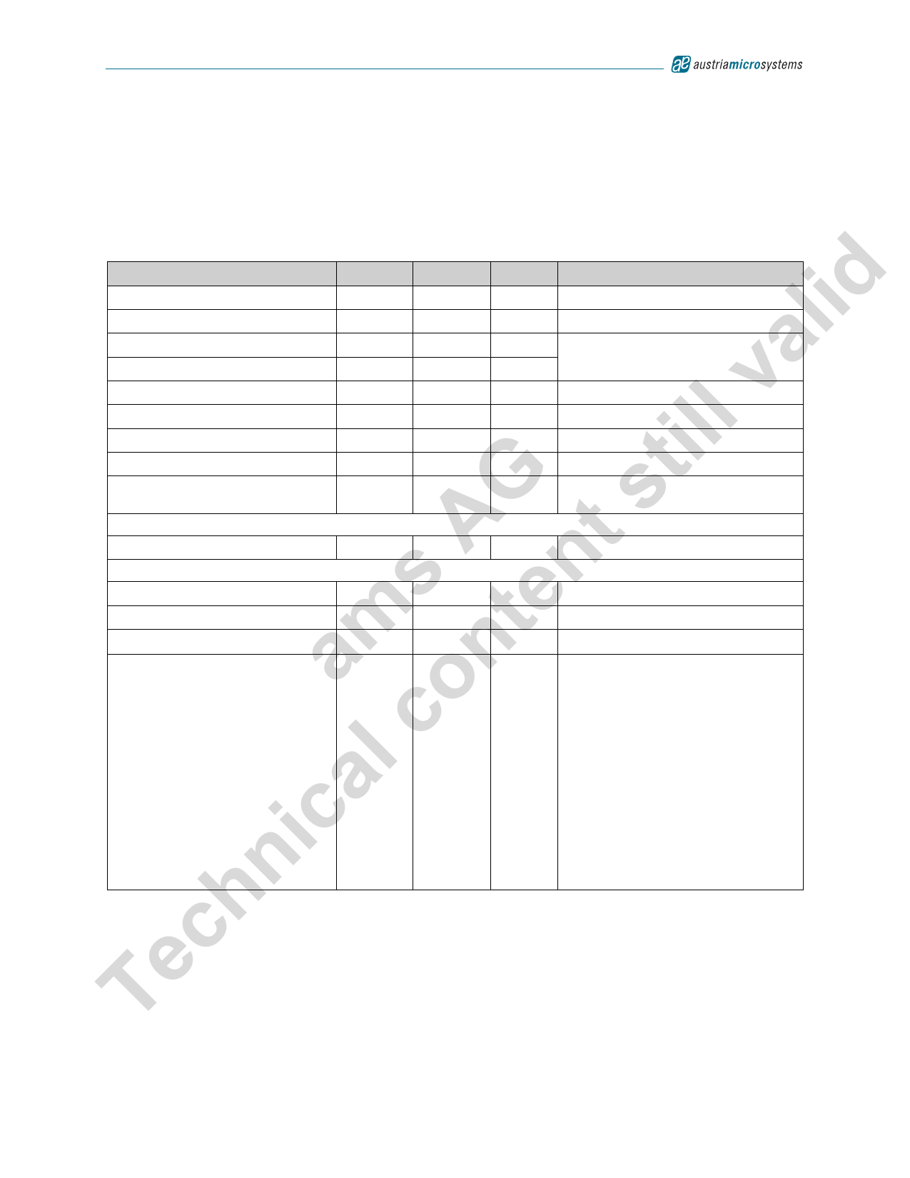
Table 2. Absolute Maximum Ratings
Parameter
Min
Max
lid VDD, PVIN to AGND
-0.3
+7
PGND to AGND
-0.3
+0.3
EN, FB, VCON
AGND - 0.3 VDD + 0.3
a SW
PGND - 0.3 PVIN + 0.3
v PVIN to VDD
-0.3
+0.3
Operating Temperature Range
-40
+85
ill Junction Temperature (TJ-MAX)
+150
Storage Temperature Range
-65
+150
t Maximum Lead Temperature
(soldering, 10sec)
+260
G s ESD Rating
A t Human Body Model
2
Operating Ratings
s n Input Voltage Range
2.7
5.5
e Recommended Load Current
650
m t Junction Temperature (TJ) Range
-40
+125
Technicaal con Ambient Temperature (TA) Range
-40
+85
Units
V
V
V
V
V
ºC
ºC
ºC
ºC
Comments
7V max
kV
HBM MIL-Std. 883E 3015.7 methods
V
mA
ºC
In applications where high power
dissipation and/or poor package thermal
resistance is present, the maximum
ambient temperature may have to be
derated.
Maximum ambient temperature (TA-MAX)
is dependent on the maximum operating
ºC
junction temperature (TJ-MAX-OP =
125ºC), the maximum power dissipation
of the device in the application (PD-MAX),
and the junction-to ambient thermal
resistance of the part/package in the
application (θJA), as given by the
following
equation: TA-MAX = TJ-MAX-OP – (θJA ×
PD-MAX).
www.austriamicrosystems.com/DC-DC_Step-Down/AS1332
Revision 1.02
3 - 19
Share Link: 