AS1302-BTDT Ver la hoja de datos (PDF) - austriamicrosystems AG
Número de pieza
componentes Descripción
Fabricante
AS1302-BTDT Datasheet PDF : 18 Pages
| |||
AS1302
Datasheet - Detailed Description
Switch Configuration
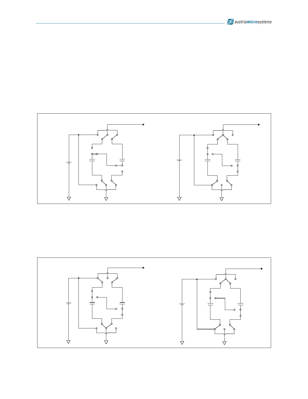
The AS1302 has nine built-in power switches in the shape of two coupled H-bridge topologies. The system features
1:2 and 2:3 operation modes as well as a 1:1 operation where the input is directly connected to the output.
In 2:3 operation mode two flying capacitors are placed in series and each capacitor is charged to the half of the input
voltage. In pumping phase the flying capacitors are placed in parallel. The bottom-plates of the parallel flying
capacitors CFLY1 and CFLY2 are connected to the input voltage so that the voltage at the top-plates of the flying
capacitors is boosted to a voltage equal to VBATT + VBATT/2. By connecting the top-plates of the capacitors to the
output, the output voltage in the 2:3 mode can be up to one and a half of VBATT. If the top-plate voltage is higher than
5V, the regulation loop adapts the power transistor’s on-resistance to drop some voltage.
Figure 33. 2:3 Operating Mode
Charging Phase
SW1
VOUT
+5V
VBATT
+2.9V to 5.15V
SW2
CFLY1
CFLY2
SW3
VBATT
+2.9V to 5.15V
SW4
Pumping Phase
SW2
SW1
VOUT
+5V
CFLY1
CFLY2
SW3
SW4
In 1:2 operation both flying capacitors are placed in parallel to the input voltage, and therefore charged to the input
voltage. During pumping phase the input voltage is connected to the bottom of the charged flying capacitors. The
voltage at the top-plates of the parallel capacitors is now boosted to 2VBATT. By connecting the top-plates of the
capacitors to the output, the output can be charged to twice the voltage of VBATT. If the top-plate voltage is higher than
5V the regulation loop limits the charge transfer to the output.
Figure 34. 1:2 Operating Mode
Charging Phase
SW1
VOUT
+5V
VBATT
+2.9V to 5.15V
SW2
CFLY1
CFLY2
SW3
VBATT
+2.9V to 5.15V
SW4
Pumping Phase
SW2
SW1
VOUT
+5V
CFLY1
CFLY2
SW3
SW4
www.austriamicrosystems.com
Revision 1.02
11 - 18
Share Link: 