APW7079 Ver la hoja de datos (PDF) - Anpec Electronics
Número de pieza
componentes Descripción
Fabricante
APW7079 Datasheet PDF : 15 Pages
| |||

APW7079
Application Information (Cont.)
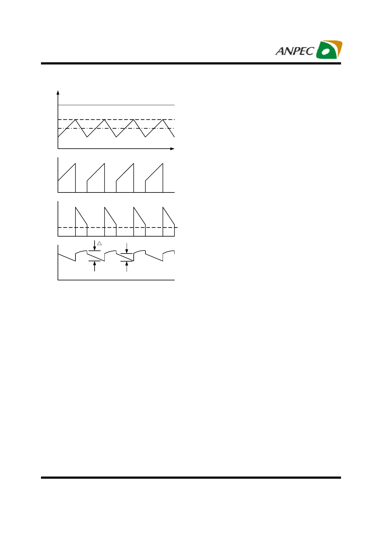
ILX
TJ = TA + TR
ILIM
where
IPEAK
T = the ambient temperature.
A
IIN
The power dissipation can be calculated as below:
PD = POUT x (1-η)/η
where
ISWN
POUT = Output power (VOUT x IOUT)
η = Efficiency
As an example, the APW7079-18 converts an input volt-
age 1.2V to provide a load current of 175mA at ambient
temperature of 85°C. Assume the efficiency (η) is 0.75.
Therefore, the power dissipated on the converter is:
ISWP
PD = 1.8 x 0.175 x (1-0.75)/0.75= 0.105 Watt
IOUT
Since the power dissipation includes the loss of external
VOUT
VOUT
IPEAK x ESR
components, the actual value is slightly lower. For the
SOT-89 package, the θJA is 180°C/W. Thus, the junction
temperature of the regulator is as below:
TJ = 85°C + (PD)(180) = 104 °C
Thermal Consideration
In most applications, the APW7079 does not dissipate
much heat due to its high efficiency. However, in applica-
tions where the APW7079 is running at high ambient tem-
perature with low output voltage, the heat dissipated may
exceed the maximum junction temperature of the part. If
the junction temperature reaches approximately 150°C,
both power switches will be turned off and the LX node
will become high impedance. To avoid the APW7079 from
exceeding the maximum junction temperature, the user
will need to do some thermal analysis. The goal of the
thermal analysis is to determine whether the power dis-
sipated exceeds the maximum junction temperature of
the part. The temperature rise is given by:
TR = (PD)(θJA)
The maximum junction temperature should be less than
125°C. Note that, the junction temperature is lower at
higher output voltages due to reduced switch resistance.
Layout Consideration
For all switching power supplies especially with high peak
currents and switching frequency, the layout is an impor-
tant step in the design. If the layout is not carefully done,
the regulator may show noise problems and duty cycle
jitter.
1.The input capacitor should be placed close to the
device, which can reduce copper trace resistance and
effect input ripple of the IC.
2.The inductor should be placed as close as possible to
the switch pin to minimize the switching noise.
3.The output capacitor should be place closed to the
VOUT and the GND.
where PD is the power dissipated by the regulator and θJA
is the thermal resistance from the junction of the die to
the ambient temperature. The junction temperature, T ,
J
is given by:
Copyright © ANPEC Electronics Corp.
10
Rev. A.3 - Oct., 2008
www.anpec.com.tw