APU1205 Ver la hoja de datos (PDF) - Advanced Power Electronics Corp
Número de pieza
componentes Descripción
Fabricante
APU1205
Advanced Power Electronics Corp

APU1205 Datasheet PDF : 4 Pages
| |||
APU1205
APU1205-18 / APU1205-25 / APU1205-28
APU1205-30 / APU1205-33 / APU1205-36
Note 1: Low duty cycle pulse testing with Kelvin con-
nections is required in order to maintain accurate data.
Note 2: Dropout voltage is defined as the minimum dif-
ferential voltage between VIN and VOUT required to main-
tain regulation at VOUT. It is measured when the output
voltage drops 1% below its nominal value.
Note 3: Ground current is the regulator quiescent cur-
rent plus the pass transistor current. The total current
from the supply is the sum of the load current plus the
ground pin current.
Note 4: The specification applies for the junction tem-
perature of 0 to +1258C.
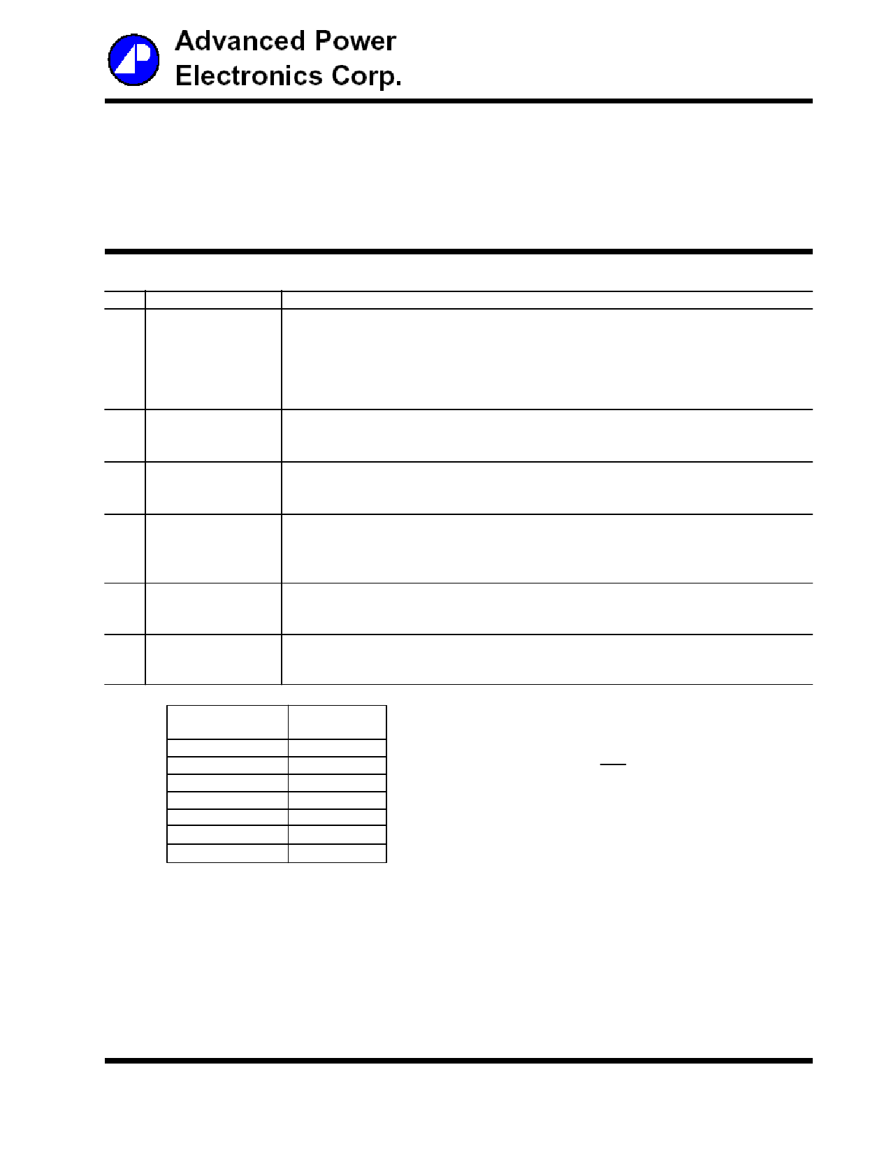
PIN DESCRIPTIONS
PIN #
1
PIN SYMBOL
VIN
PIN DESCRIPTION
The input pin of the regulator. Typically a large storage capacitor is connected from
this pin to ground to insure that the input voltage does not sag below the minimum
drop out voltage during the load transient response. This pin must always be higher
than VOUT by at least the amount of the dropout voltage and some margin in order for
the device to regulate properly.
2
Gnd
Ground pin. This pin must be connected to the lowest potential in the system and all
other pins must be at higher potential with respect to this pin.
3
En
Enable pin. A low signal or left open on this pin shuts down the output. This pin must
be tied HI or to VIN for normal operation.
4
Adj
A resistor divider from this pin to the VOUT pin and ground sets the output voltage. To
(Adjustable Only) minimize the error due to the error amplifier, select the values of the resistor dividers
to be less than 10KV.
4
CBYP
A 470 to 1000pF bypass capacitor connected to this pin reduces the output noise.
(Fixed Only)
5
VOUT
The output of the regulator. A minimum of 2.2mF with max ESR of 1V capacitor must
be connected from this pin to ground to insure stability.
5-PIN
SOT-23
APU1205
APU1205-18
APU1205-25
APU1205-28
APU1205-30
APU1205-33
APU1205-36
Output
Voltage
1.25V
1.8V
2.5V
2.8V
3.0V
3.3V
3.6V
Table 1- Nominal output voltage vs. part number.
The output voltage of the adjustable device can be set
using:
( ) Vo = 1.253
1+
R1
R2
Where:
R1 = Resistor connected from output to the Adj pin
R2 = Resistor connected from Adj pin to Gnd
3/4
Share Link: