CA3080(1998) Ver la hoja de datos (PDF) - Intersil
Número de pieza
componentes Descripción
Fabricante
CA3080 Datasheet PDF : 11 Pages
| |||
CA3080, CA3080A
Absolute Maximum Ratings
Thermal Information
Supply Voltage (Between V+ and V- Terminal) . . . . . . . . . . . . . 36V
Differential Input Voltage . . . . . . . . . . . . . . . . . . . . . . . . . . . . . . . 5V
Input Voltage . . . . . . . . . . . . . . . . . . . . . . . . . . . . . . . . . . . . V+ to V-
Input Signal Current . . . . . . . . . . . . . . . . . . . . . . . . . . . . . . . . . . 1mA
Amplifier Bias Current (IABC) . . . . . . . . . . . . . . . . . . . . . . . . . . . 2mA
Output Short Circuit Duration (Note 1). . . . . . . . . . . . . No Limitation
Operating Conditions
Temperature Range
CA3080 . . . . . . . . . . . . . . . . . . . . . . . . . . . . . . . . . . . 0oC to 70oC
CA3080A . . . . . . . . . . . . . . . . . . . . . . . . . . . . . . . . -55oC to 125oC
Thermal Resistance (Typical, Note 2)
θJA (oC/W) θJC (oC/W)
PDIP Package . . . . . . . . . . . . . . . . . . . 130
N/A
SOIC Package . . . . . . . . . . . . . . . . . . . 170
N/A
Metal Can Package . . . . . . . . . . . . . . . 200
120
Maximum Junction Temperature (Metal Can). . . . . . . . . . . . . . 175oC
Maximum Junction Temperature (Plastic Package) . . . . . . . 150oC
Maximum Storage Temperature Range . . . . . . . . . . -65oC to 150oC
Maximum Lead Temperature (Soldering 10s) . . . . . . . . . . . . 300oC
(SOIC - Lead Tips Only)
CAUTION: Stresses above those listed in “Absolute Maximum Ratings” may cause permanent damage to the device. This is a stress only rating and operation of the
device at these or any other conditions above those indicated in the operational sections of this specification is not implied.
NOTES:
1. Short circuit may be applied to ground or to either supply.
2. θJA is measured with the component mounted on an evaluation PC board in free air.
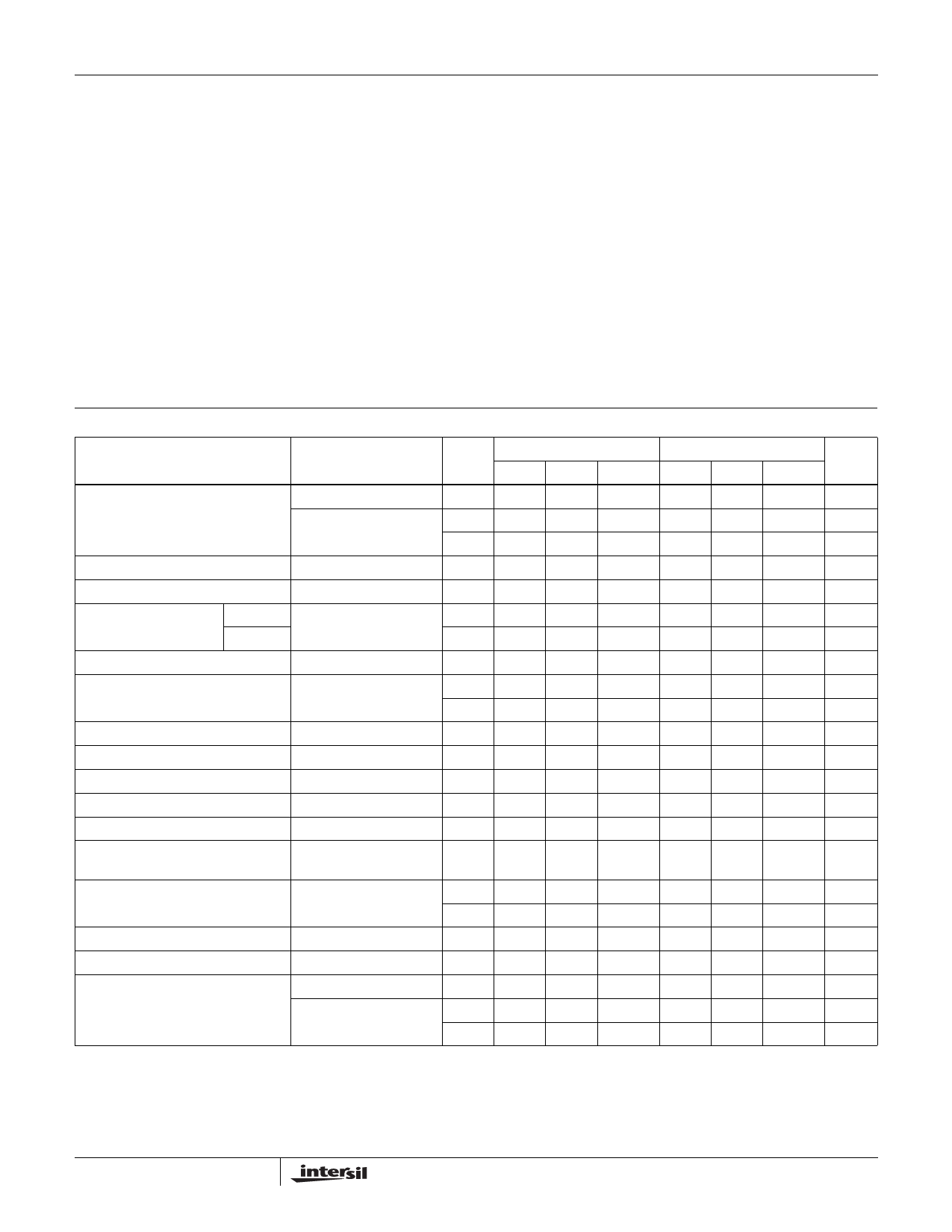
Electrical Specifications For Equipment Design, VSUPPLY = ±15V, Unless Otherwise Specified
CA3080
PARAMETER
TEST CONDITIONS TEMP MIN TYP MAX
Input Offset Voltage
IABC = 5µA
IABC = 500µA
25
-
0.3
-
25
-
0.4
5
Full
-
-
6
Input Offset Voltage Change
Input Offset Voltage Temp. Drift
Input Offset Voltage
Sensitivity
Positive
Negative
IABC = 500µA to 5µA
IABC = 100µA
IABC = 500µA
25
-
0.2
-
Full
-
-
-
25
-
-
150
25
-
-
150
Input Offset Current
Input Bias Current
IABC = 500µA
IABC = 500µA
25
-
0.12
0.6
25
-
2
5
Full
-
-
7
Differential Input Current
Amplifier Bias Voltage
Input Resistance
Input Capacitance
Input-to-Output Capacitance
Common-Mode Input-Voltage
Range
IABC = 0, VDIFF = 4V
25
-
0.008
-
IABC = 500µA
25
-
0.71
-
IABC = 500µA
25
10
26
-
IABC = 500µA, f = 1MHz
25
-
3.6
-
IABC = 500µA, f = 1MHz
25
-
0.024
-
IABC = 500µA
25 12 to 13.6 to
-
-12 -14.6
Forward Transconductance
(Large Signal)
IABC = 500µA
25 6700 9600 13000
Full 5400
-
-
Output Capacitance
Output Resistance
Peak Output Current
IABC = 500µA, f = 1MHz
25
-
5.6
-
IABC = 500µA
25
-
15
-
IABC = 5µA, RL = 0Ω
25
-
5
-
IABC = 500µA, RL = 0Ω
25
350 500
650
Full 300
-
-
MIN
-
-
-
-
-
-
-
-
-
-
-
-
10
-
-
12 to
-12
7700
4000
-
-
3
350
300
CA3080A
TYP MAX
0.3
2
0.4
2
-
5
0.1
3
3.0
-
-
150
-
150
0.12
0.6
2
5
-
15
0.008
5
0.71
-
26
-
3.6
-
0.024
-
13.6 to
-
-14.6
9600 12000
-
-
5.6
-
15
-
5
7
500
650
-
-
UNITS
mV
mV
mV
mV
µV/oC
µV/V
µV/V
µΑ
µA
µA
nA
V
kΩ
pF
pF
V
µS
µS
pF
MΩ
µA
µA
µA
2
Share Link: 