APL5930 Ver la hoja de datos (PDF) - Anpec Electronics
Número de pieza
componentes Descripción
Fabricante
APL5930 Datasheet PDF : 17 Pages
| |||
APL5930
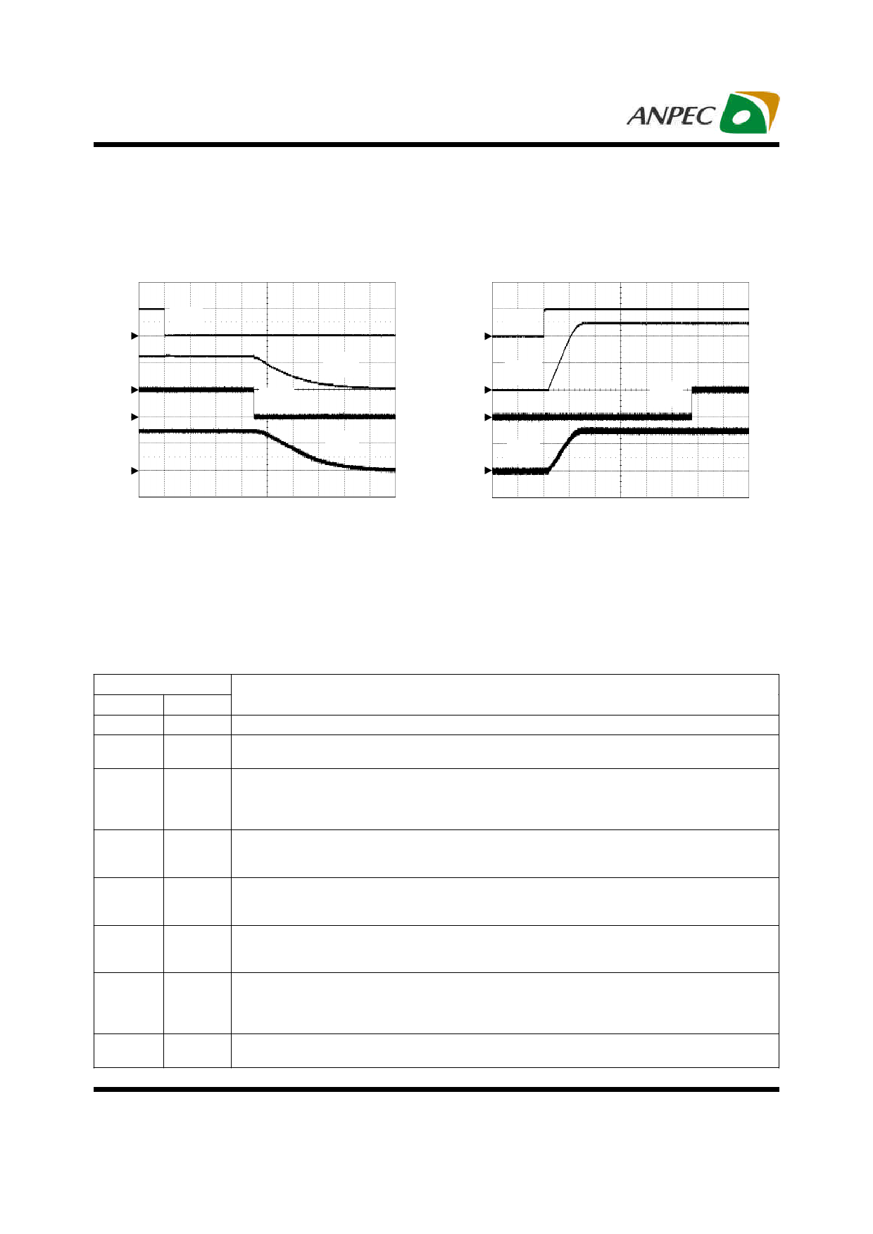
Operating Waveforms (Cont.)
Refer to the typical application circuit. The test condition is VIN=1.8V, VCNTL=5V, VOUT=1.2V, TA= 25oC
unless otherwise specified.
Shutdown
Enable
VEN
1
2
3
4
VPOK
VOUT
IOUT
COUT=10µF, CIN=10µF, RL=0.4Ω
CH1: VEN, 5V/Div, DC
CH2: VOUT, 1V/Div, DC
CH3: VPOK, 5V/Div, DC
CH4: IOUT, 2A/Div, DC
TIME: 2µs/Div
VEN
1
VOUT
2
3
IOUT
4
VPOK
COUT=10µF, CIN=10µF, RL=0.4Ω
CH1: VEN, 5V/Div, DC
CH2: VOUT, 0.5V/Div, DC
CH3: VPOK, 5V/Div, DC
CH4: IOUT, 2A/Div, DC
TIME: 0.5ms/Div
Pin Description
PIN
NO.
NAME
1
GND
2
FB
3,4
VOUT
5
VIN
6
VCNTL
7
POK
8
EN
Exposed
Pad
-
FUNCTION
Ground pin of the circuitry. All voltage levels are measured with respect to this pin.
Voltage Feedback Pin. Connecting this pin to an external resistor divider receives the feedback voltage
of the regulator.
Output pin of the regulator. Connecting this pin to load and output capacitors (10µF at least) is required
for stability and improving transient response. The output voltage is programmed by the resistor-divider
connected to FB pin. The VOUT can provide 3A (max.) load current to loads. During shutdown, the
output voltage is quickly discharged by an internal pull-low MOSFET.
Main supply input pin for voltage conversions. A decoupling capacitor (≥10µF recommended) is usually
connected near this pin to filter the voltage noise and improve transient response. The voltage on this
pin is monitored for Power-On-Reset purpose.
Bias voltage input pin for internal control circuitry. Connect this pin to a voltage source (+5V
recommended). A decoupling capacitor (1µF typical) is usually connected near this pin to filter the
voltage noise. The voltage at this pin is monitored for Power-On-Reset purpose.
Power-OK signal output pin. This pin is an open-drain output used to indicate the status of output
voltage by sensing FB voltage. This pin is pulled low when output voltage is not within the Power-OK
voltage window.
Active-high enable control pin. Applying and holding the voltage on this pin below the enable voltage
threshold shuts down the output. When re-enabled, the IC undergoes a new soft-start process. When
leave this pin open, an internal pull-up current (5µA typical) pulls the EN voltage and enables the
regulator.
Connect this pad to system VIN plane for good thermal conductivity.
Copyright © ANPEC Electronics Corp.
8
Rev. A.4 - Sep., 2009
www.anpec.com.tw
Share Link: 