APL5913 Ver la hoja de datos (PDF) - Anpec Electronics
Número de pieza
componentes Descripción
Fabricante
APL5913 Datasheet PDF : 19 Pages
| |||

APL5913
Application Information (Cont.)
Feedback Network (Cont.)
Select a proper R1(selected) to be a little larger
than the calculated R1.
- Calculate the C1 as the following :
[ ] C1(pF) = 0.71⋅ ESR(mΩ) + 101 ⋅ COUT(uF) ........ (4)
R1(kΩ )
Where R1=R1(selected)
Select a proper C1(selected) to be a little smaller
than the calculated C1.
- The C1 calculated from equation (4) must meet
the following equation:
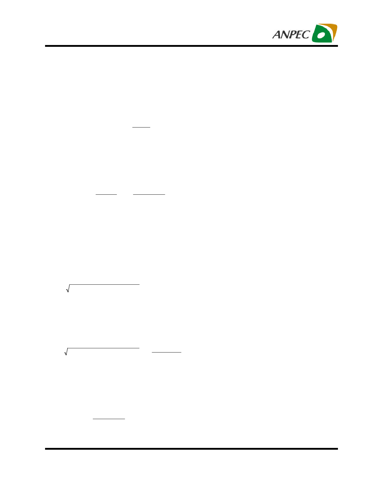
C1 (pF)
≥
7.2
⋅ 1+
143
ESR (m
Ω
)
⋅
1
+
37.5 ⋅ VOUT(V)
R1 (kΩ)
..
(5)
Where R1=R1(calculated) from equation (3)
If the C1(calculated) can not meet the equation (8),
please use the Condition 2.
- Use equation (2) to calculate the R2.
The reason to have three conditions described above
is to optimize the load transient responses for all kinds
of the output capacitor. For stability only, the Condition
2, regardless of equation (5), is enough for all kinds of
output capacitor.
PCB Layout Considerations (See Figure 2)
1. Please solder the Exposed Pad and VIN together
on the PCB. The main current flow is through the
exposed pad. Refer Figure 3 to make a proximate
topology.
If the C1(calculated) can not meet the equation
(5), please use the Condition 3.
2. Please place the input capacitors for VIN and
VCNTL pins near pins as close as possible.
- Use equation (2) to calculate the R2.
•Condition 3 : Low ESR (eg. Ceramic Capacitors)
3. Ceramic decoupling capacitors for load must be
placed near the load as close as possible.
4. To place APL5913 and output capacitors near the
- Calculate the R1 as the following:
load is good for performance.
R1(kΩ) = (2.1⋅ESR(mΩ) + 300)⋅ COUT(uF) − 37.5⋅ VOUT(V).. (6)
5. The negative pins of the input and output capaci-
tors and the GND pin of the APL5913 are connected
Select a proper R1(selected) to be a little larger to the ground plane of the load.
than the calculated R1. The minimum selected 6. Please connect PIN 3 and 4 together by a wide
R1 is equal to 1kΩ when the calculated R1 is track.
smaller than 1k or negative.
- Calculate the C1 as the following :
C1(pF) =
(0.24⋅ESR(mΩ)
+
34.2)⋅
COUT(uF) ⋅
1+
37.5⋅ VOUT(V)
R1(kΩ)
..
(7)
Where R1=R1(selected)
7. Large current paths must have wide tracks.
8. See the Typical Application
(see next page Figure 2)
- Connect the one pin of the R2 to the GND of
Select a proper C1(selected) to be a little smaller
than the calculated C1.
APL5913
- Connect the one pin of R1 to the Pin 3 of APL5913
- The C1 calculated from equation (7) must meet
- Connect the one pin of C1 to the Pin 3 of APL5913
the following equation :
C1 (pF)
≥
0.033
+
1.25 ⋅ VOUT(V)
R1 (kΩ )
⋅
ESR
(m
Ω
)
⋅
C OUT(uF)
.. (8)
Where R1=R1(calculated) from equation (6)
Copyright © ANPEC Electronics Corp.
14
Rev. A.4 - May., 2005
www.anpec.com.tw