MR27V3266D Ver la hoja de datos (PDF) - Oki Electric Industry
Número de pieza
componentes Descripción
Fabricante
MR27V3266D Datasheet PDF : 36 Pages
| |||
1 Semiconductor
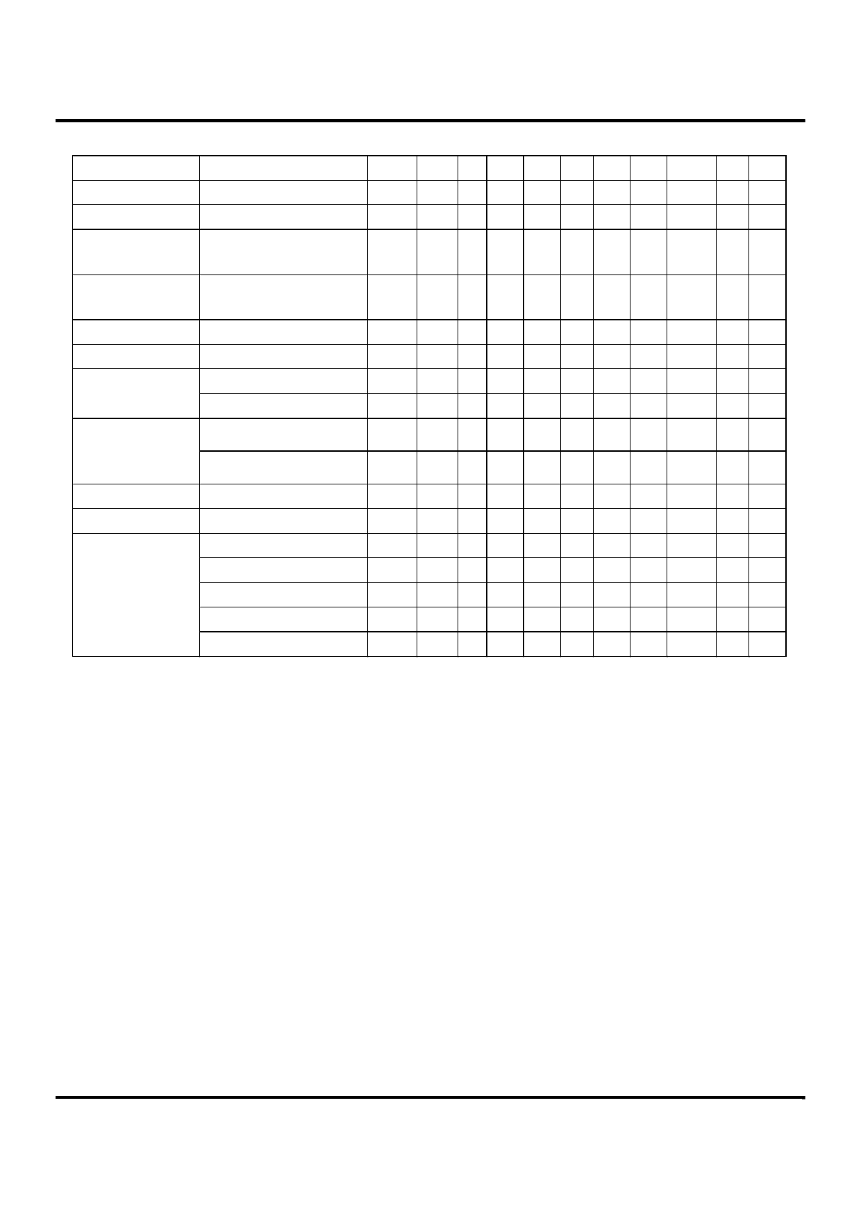
FUNCTION TABLE FOR SYNCHRONOUS READ
MR27V3266D
COMMAND NAME
Mode Register Set
Row Active
Read Word
(x16)
FUNCTION
Mode Register Set
Row Address Latch
Column Address Latch
Trigger Burst Read
CKEn-1 CKEn /CS /RAS /CAS /MR DQM Add. /WORD STO Notes
H X L L L L X Code X L 1
H X L L H H X RA X L 2
H X L H L H X CA L L 3
Read Double Word Column Address Latch
(x32)
Trigger Burst Read
H X L H L H X CA H L 3
Burst Stop
Burst Stop
Precharge
Burst Stop
Clock Suspend
(on Read)
Entry
Exit
Power Down
(on Active
Entry
Standby) Exit
H X LH HL X X X L 4
H XLL HLX X X L 4
H L XX XX X X X L 5
L HXX XX X X X L 5
H L HX X X X X X L 6
L HXX XX X X X L 6
Read Output
Output Enable
H XXX XX L X X L
Mask Output
High-Z Output
H XXX XXH X X L
No Operation
Write on SDRAM
H X LH L L X X X L
Self Refresh on SDRAM
H L LL LHX X X L
Illegal on SDRAM
H HLL LHX X X L
H X HX X X X X X L
H X LH HHX X X L
( H=Logical high, L=Logical low, X=Don't Care, L of STO includes pin open due to internal pull down resistor )
Note
( CKEn expresses the logical level at the simultaneous cycle with a command. )
1. Refer to "Mode register Field Table" for Address Codes, and Mode Transition Chart for operational state.
After power on any command can be sampled at any cycle in Active Standby state.
After "Mode register Set" command is sampled, no new command can be accepted for 3 CLK cycles.
The /CS input must be kept high for the 3 CLK cycles to prevent unexpected sampling of a command.
2. The "Row Active" command is effective till new "Row Active" command is implemented.
3. The /WORD input is sampled simultaneously with "Read" command to select data width.
A Double Word Burst(x32 ) or a Word Burst(x16) is selected by the /WORD input for each "Read" command.
On condition of constant voltage level on /Word pin, organization is fixed to either x16 or x32.
"Read" command ends it's implementation by itself at the finishing cycle of the burst read.
4. Since OTP technology uses static sense amplifiers, the "Precharge" command is not required however,
due to customer request for the similarity of logical input code with SDRAM command, the name of
"Precharge" is adopted. Function of "Precharge" command and "Burst Stop" command is only to stop the burst
read cycles delayed by CAS Latency.
5. Sampled low level CKE disables CLK buffer to suspend internal clock signals at the next rising edge of CLK.
Sampled high level CKE enables internal clock at the next rising edge of CLK.
Low level CKE sampled in the period from the simultaneous cycle with a "Read" command till the end of the
burst read cycle is distinguished with internal command controller from the low level CKE sampled in Active
Standby state not to stop data sensing and burst read operation those consume power.
6. Low level CKE sampled in Active Standby state cuts power dissipation to be in Power Down state.
High level CKE sampled in Power Down state enables internal CKE to be in Active Standby state with
preserved row address.
August , 1999
Revision 2.4
32M Synchronous OTP
6
Share Link: 