APA4838 Ver la hoja de datos (PDF) - Anpec Electronics
Número de pieza
componentes Descripción
Fabricante
APA4838
Anpec Electronics

APA4838 Datasheet PDF : 29 Pages
| |||
APA4838
Application Descriptions
BTL Operation
BTL Operation (Cont.)
The APA4838 output stage (power amplifier) has two A BTL amplifier design has a few distinct advantages
pairs of operational amplifiers internally, allowed for over the SE configuration, as it provides differential
different amplifier configurations for each channel. drive to the load, thus doubling the output swing for a
Gain 1
Gain 2
specified supply voltage.
Four times the output power is possible as compared
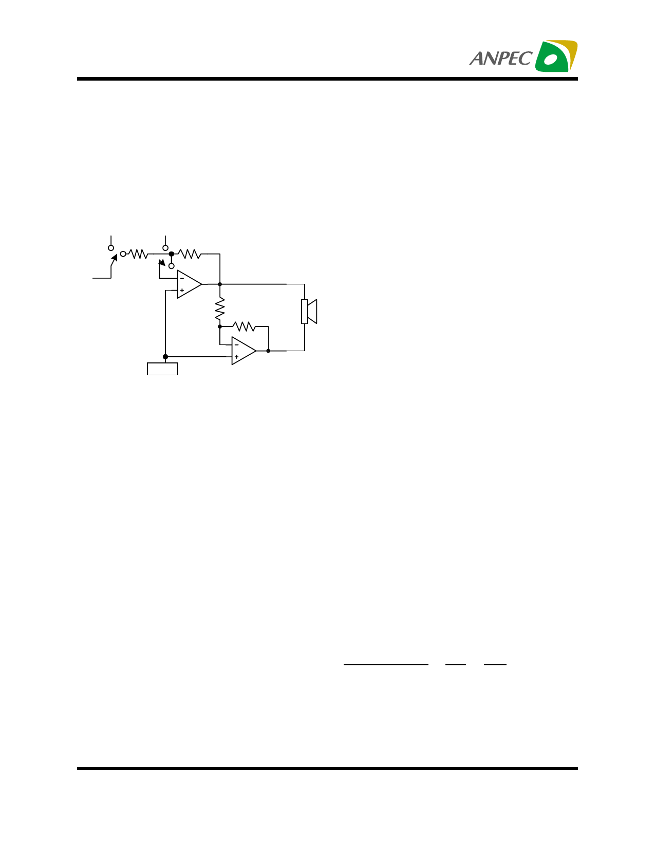
Volume Control
Am plifier output signal
OP1
-Out
to a SE amplifier under the same conditions. A BTL
configuration, such as the one used in APA4838, also
creates a second advantage over SE amplifiers.
RL Since the differential outputs, +Right Out, -Right Out,
+Out
+Left Out, and -Left Out, are biased at half-supply,
Vbias
OP2
no need DC voltage exists across the load. This elimi-
Figure 1: APA4838 power amplifier internal configu- nates the need for an output coupling capacitor which
ration (each channel)
is required in a single supply, SE configuration.
The power amplifier OP1 gain is setting by internal
unity-gain or external gain setting which is selected
from Gain Select pin and the audio input signal come
from internal volume control block, while the second
amplifier OP2 is internally fixed in a unity-gain, in-
verting configuration. Figure 1 shows that the output
of OP1 is connected to the input to OP2, which re-
sults in the output signals of with both amplifiers with
identical in magnitude, but out of phase 180°.
Consequently, the differential gain for each channel
is 2X (Gain of SE mode).
By driving the load differentially through outputs -Out
Single-Ended Operation
Consider the single-supply SE configuration shown
Application Circuit. A coupling capacitor is required
to block the DC offset voltage from reaching the load.
These capacitors can be quite large (approximately
33µF to 1000µF) so they tend to be expensive, oc-
cupy valuable PCB area, and have the additional
drawback of limiting low-frequency performance of
the system (refer to the Output Coupling Capacitor).
The rules described still hold with the addition of the
following relationship:
and +Out, an amplifier configuration commonly re-
ferred to as bridged mode is established. BTL mode
1
Cbypass x 125kΩ
≤
1 << 1
RiCi RLCC
(1)
operation is different from the classical single-ended
SE amplifier configuration where one side of its load
is connected to ground.
Copyright ANPEC Electronics Corp.
17
Rev. A.1 - Apr., 2003
www.anpec.com.tw
Share Link: