AP602 Ver la hoja de datos (PDF) - WJ Communications => Triquint
Número de pieza
componentes Descripción
Fabricante
AP602 Datasheet PDF : 11 Pages
| |||
AP602
High Dynamic Range 4W 28V HBT Amplifier
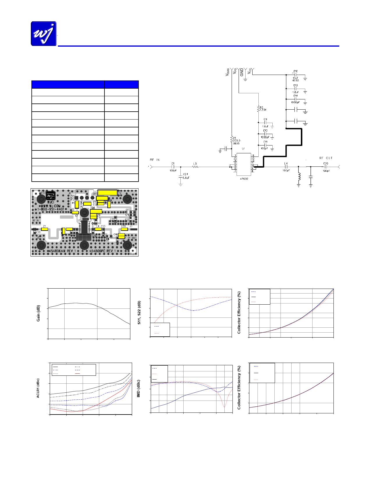
869-960 Application Circuit (AP602-PCB900)
Typical WCDMA Performance at 25 °C
at a channel power of +27 dBm
Frequency
940 MHz
W-CDMA Channel Power
+27 dBm
Power Gain
15.5 dB
Input Return Loss
11 dB
Output Return Loss
6.4 dB
ACLR
-50 dBc
IMD3 @ +27 dBm PEP
-50 dBc
Operating Current, Icc
103 mA
Collector Efficiency
17 %
Output P1dB
+35.7 dBm
Quiescent Current, Icq
80 mA
Vpd, Vbias
+5 V
Vcc
+28 V
2 Ohm
See note 4
C7
1000pF
C15
100pF
C30
100pF
W = .030”
L = 1.570”
L10
8.2 nH
See note 5
C19
0.4 pF
See note 6
Notes:
1. The primary RF microstrip line is 50 Ω.
2. Components shown on the silkscreen but not on the schematic are not used.
C30
3. C20 is not required in the final design if there is no DC signal present at the output of the
amplifier circuit.
4. The center of C24 is placed at 0.280” (11.5° @ 940 MHz) from the edge of the AP602 (U1).
C24 L3
5. The center of L10 is placed at 0.570” (23.4° @ 940 MHz) from the edge of the AP602 (U1).
6. The center of C19 is placed at 0.050” (2.1° @ 940 MHz) the center of L10.
L10
7. The bold-faced RF trace is for the DC bias feed. The stub’s length is approximately a ¼ λ.
8. The main RF trace is cut at component L3 and L4 for this particular reference design.
869-960 MHz Application Circuit Performance Plots
Gain vs. Frequency
Vcc = 28V, Icq = 80 mA, 25 ˚C
18
17
16
S11, S22 vs. Frequency
Vcc = 28V, Icq = 80 mA, 25 ˚C
0
-5
-10
Efficiency vs. Output Power vs. Frequency
CW tone, Vcc = 28V, Icq = 80 mA, 25 ˚C
50
920 MHz
40
940 MHz
960 MHz
30
15
14
13
0.8
0.84 0.88 0.92 0.96
1
Frequency (GHz)
ACLR1 vs. Output Power vs. Frequency
-42
WCDMA, Vcc= 28V, Icq = 40mA, 25oC
-46
869MHz
894MHz
940MHz
880MHz
920MHz
960MHz
WCDMA 3GPP TM 1+64 DPCH;
PAR = 8.6 @0.01%
60% clipping, Ch. BW = 3.84 MHz;
-50
-54
-58
-62
18
20
22
24
26
28
Output Power (dBm)
-15
-20
-25
0.8
S11
S22
0.85
0.9
0.95
1
Frequency (GHz)
1.05
1.1
IMD vs. Output Power
CW 2-tone signal, 940 MHz, ∆f = 1 MHz, 28V, 80 mA Icq, 25 ˚C
-40
IMD3L
IMD3U
-50
IMD5
-60
-70
-80
22
24
26
28
30
32
Output Power, PEP (dBm)
20
10
0
18
25
20
15
22
26
30
34
Output Power (dBm)
Efficiency vs. Output Power vs. Frequency
WCDMA, Vcc = 28V, Icq = 80 mA, 25 ˚C
920 MHz
940 MHz
960 MHz
10
5
0
18
20
22
24
26
28
Average Output Power (dBm)
Unconditionally stable version of this application circuit is available for download off of the website at: http://www.wj.com
Specifications and information are subject to change without notice
WJ Communications, Inc • Phone 1-800-WJ1-4401 • FAX: 408-577-6621 • e-mail: sales@wj.com • Web site: www.wj.com
Page 4 of 11 May 2007 ver 1
Share Link: 