AP3703 Ver la hoja de datos (PDF) - BCD Semiconductor
Número de pieza
componentes Descripción
Fabricante
AP3703 Datasheet PDF : 11 Pages
| |||
Preliminary Datasheet
LOW-POWER OFF-LINE PRIMARY SIDE REGULATION CONTROLLER AP3703
Operation Description (Continued)
where the Vd is the diode forward drop voltage.
See equation 5
The relationship between the output constant-current
and secondary peak current Ipks is given by:
Iout = 1 × Ipks× Tons
2
Tons+ Toffs
......(7)
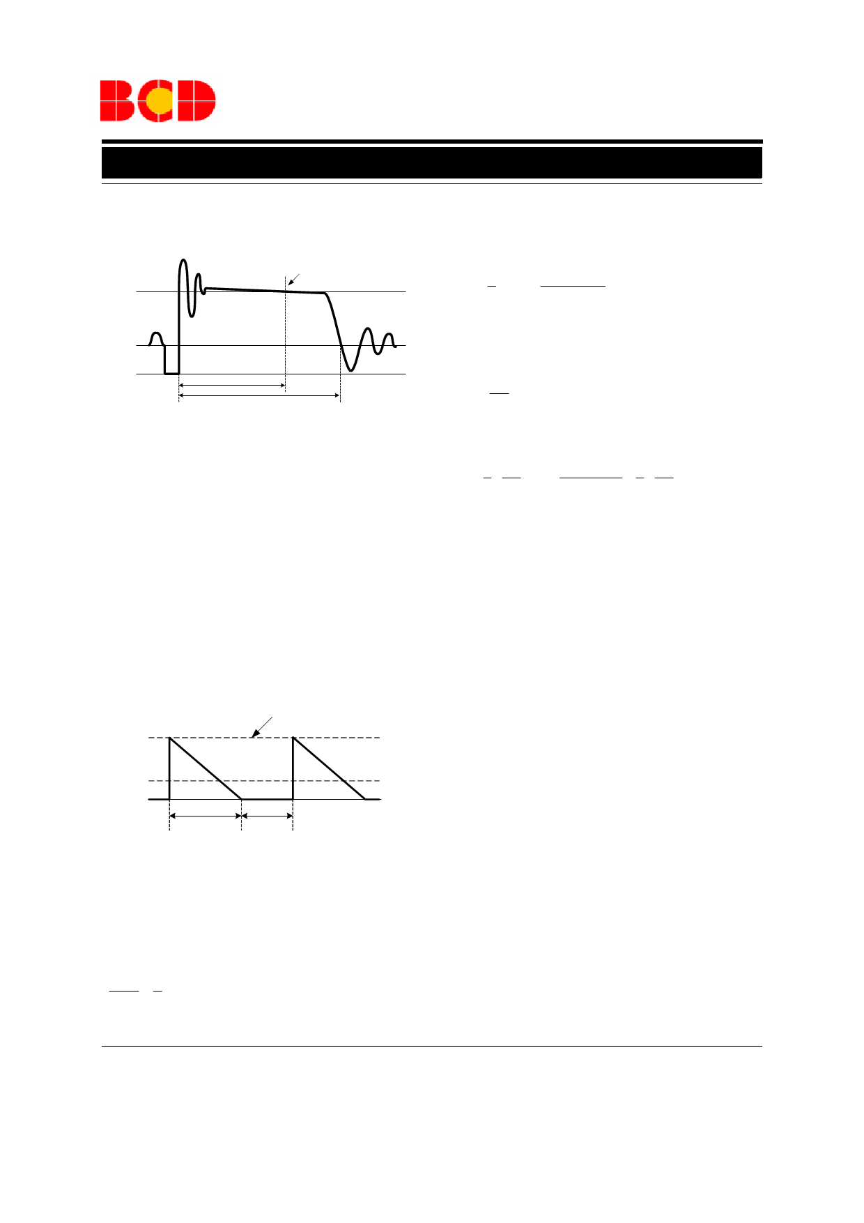
0V
2/3 Tons
Tons
Figure 9. Auxiliary Voltage Waveform
The output voltage is different from the secondary
voltage in a diode forward drop voltage that depends
on the current. If the secondary voltage is always
detected at a fixed secondary current, the difference
between the output voltage and the secondary voltage
will be a fixed Vd. For AP3703, the voltage detection
point is at two-thirds of the D1 on-time, which means
the the secondary voltage is detected at a fixed
secondary current of one-third of Ipks. The CV loop
control function of AP3703 then generates a D1 off-
time to regulate the output voltage.
Constant Current Operation
Figure 10 shows the secondary current waveforms.
See equation 8
Is
Iout
0A
Tons
Toffs
Figure 10. Secondary Current Waveform
In CC operation, the CC loop control function of
AP3703 will keep a fixed proportion between D1 on-
time Tons and D1 off-time Toffs by discharging or
charging a capacitor embedded in the IC. The fixed
proportion is:
Tons = 4
Toffs 3
......(6)
At the instant of D1 turn-on, the primary current
transfers to the secondary at an amplitude of:
Ipks = NP × Ipk
NS
......(8)
Thus the output constant-current is given by:
Iout = 1 × NP × Ipk× Tons = 2 × NP × Ipk ......(9)
2 NS
Tons+ Toffs 7 NS
Leading Edge Blanking
When the power switch is turned on, a turn-on spike
will occur on the sense-resistor. To avoid false-
termination of the switching pulse, a 430ns leading-
edge blanking is built in. During this blanking period,
the current sense comparator is disabled and the gate
driver can not be switched off.
CCM Protection
The AP3703 is designed to operate in discontinuous
conduction mode (DCM) in both CV and CC modes.
To avoid operating in continuous conduction mode
(CCM), the AP3703 detects the falling edge of the FB
input voltage on each cycle. If a 0.1V falling edge of
FB is not detected, the AP3703 will stop switching.
OVP & OCkP
The AP3703 includes output over-voltage protection
(OVP) and open circuit protection (OCkP) circuitry as
shown in Figure 11. If the voltage at FB pin exceeds
8V, 100% above the normal detection voltage, or the
-1.5V falling edge of the FB input can not be
monitored, the AP3703 will immediately shut off and
enters hiccup mode. The AP3703 sends out a fault
detection pulse every 24ms in hiccup mode until the
fault has been removed.
Feb. 2009 Rev. 1.0
BCD Semiconductor Manufacturing Limited
8
Share Link: 