AP2218T-5.0E1 Ver la hoja de datos (PDF) - BCD Semiconductor
Número de pieza
componentes Descripción
Fabricante
AP2218T-5.0E1 Datasheet PDF : 13 Pages
| |||
Preliminary Datasheet
1A LOW DROPOUT LINEAR REGULATOR
AP2218
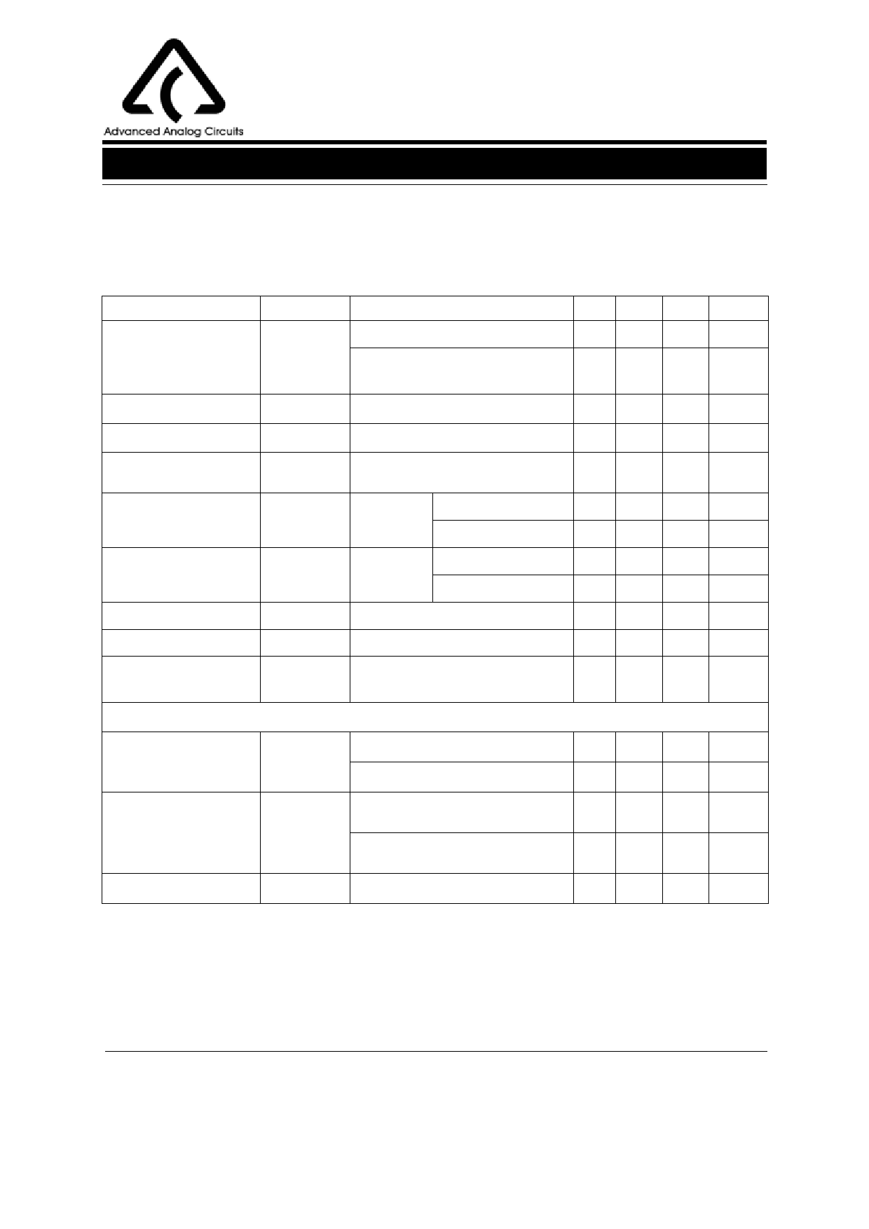
Electrical Characteristics (Continued)
AP2218-5.0V Electrical Characteristics
Operating Conditions: VIN=6V, CIN=10µF, COUT=10µF, TJ=25oC, unless otherwise specified. The Boldface
applies over -40oC≤TJ≤125oC. (P≤maximum power dissipation.)
Parameter
Output Voltage
Line Regulation
Load Regulation
Output Voltage
Temperature Coefficient
Dropout Voltage (Note 3)
Ground Current
Current Limit
Minimum Load Current
Output Noise Voltage (rms)
Enable Input
Symbol
VOUT
VRLINE
VRLOAD
∆VOUT/∆T
Condition
IOUT=10mA
10mA≤IOUT≤1A, 6V≤VIN≤8V
(Note 2)
IOUT=10mA, 6V≤VIN≤8V
VIN=6V, 10mA≤IOUT≤1A
IOUT=10mA
VDROP
IGND
ILIMIT
ILOAD(MIN)
∆VOUT=1% IOUT=100mA
IOUT=1A
VIN=6V
IOUT=750mA
IOUT=1A
VOUT=0V (Note 4)
10Hz to 100KHz, IOUT=100mA,
COUT=10µF
Min Typ Max Unit
4.95 5.0 5.05
V
4.90
5.10
V
5
50
mV
10 75
mV
100 500 µV/oC
70 200 mV
300 550 mV
6
15
mA
10
mA
1.5 2.2
A
1
5
mA
400
µV
Enable Input Voltage
VEN
Logic low (off)
Logic high (on)
0.8
V
2.25
V
Enable Input Current
IIN
VEN=2.25V
VEN=0.8V
Shutdown Output Current IOUT(SHDN) (Note 5)
1
15 30
µA
75
2
µA
4
10 20
µA
Note 2: For the details of VIN range, please refer to (VIN-VOUT)*ILOAD≤maximum power dissipation (Figure 4).
Note 3: Dropout voltage is defined as the input-to-output differential when the output voltage drops to 99% of its nominal value
which is measured at VOUT+1V applied to VIN.
Note 4: VIN=VOUT(NOMINAL)+1V.
Note 5: VEN ≤0.8V, VIN≤8V, VOUT=0V.
Aug. 2005 Rev. 1. 0
BCD Semiconductor Manufacturing Limited
6
Share Link: 