AP1127D Ver la hoja de datos (PDF) - Anachip Corporation
Número de pieza
componentes Descripción
Fabricante
AP1127D Datasheet PDF : 4 Pages
| |||
3A Bus Terminator Regulator
AP1127
Electrical Characteristics
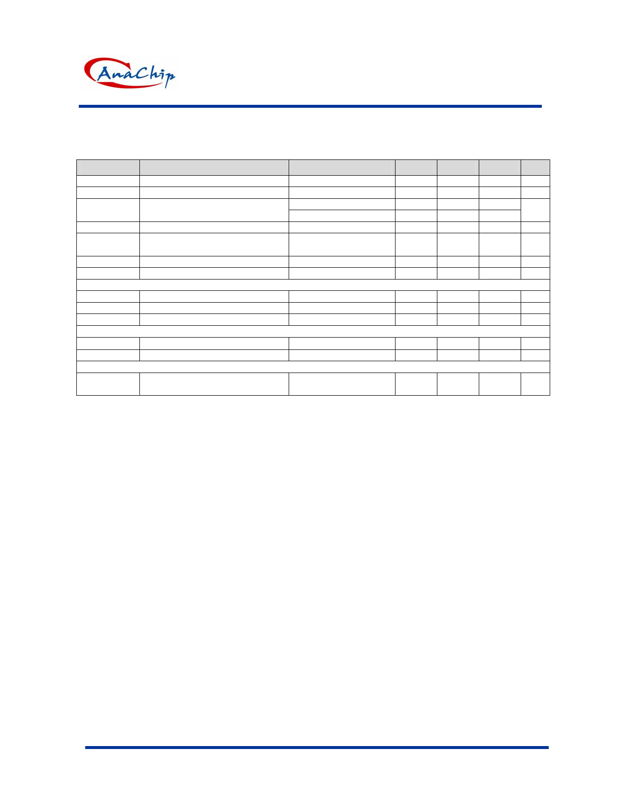
Unless otherwise stated, these specifications apply TA=25oC; VIN=+2.5V and VCCA=+3.3V, VREFEN=1.25V) maximum ratings are stress
ratings only and functional device operating is not implied. (Note 1)
Symbol
Parameter
Conditions
Min. Typ. Max. Unit
VOS
Output Offset Voltage
IOUT=0A (Note 2)
-20
-
20 mV
IOP
Operating Current at VIN
No load, COUT=200uF
-
-
1
mA
∣∆VLOAD∣ Load Regulation (DDR I/II)
IL: 0A~3A
IL: 0A~3A
-
-
0.8/1.2 2/3
0.8/1.2 2/3
%
ICCQ
Quiescent Current at VCCA
At room temp.
-
190
230 µA
ISHDN
VIN
VCCA
Current in Shutdown Mode
Input Voltage Range (Note 3)
Input Voltage Range (Note 3)
REFEN < 0.2V,
RL=10Ω
No load
RL=10Ω
-
90
110 µA
1.35/1 2.5/1.8 6
V
3.75
-
6
V
Short Circuit Protection
ILIMIT
ISC, VIN
ISC, GND
Current Limit
Short Current
Short Current
Sinking
Sourcing
-
5
-
A
2
-
-
A
3
-
-
A
Over Thermal Protection
THSD Thermal Shutdown Temperature 3.75V ≤ VCCA ≤ 6V
Thermal Shutdown Hysteresis
125
150
25
30
-
oC
35
oC
REFEN Function
REFEN Threshold
VREFEN < VIN
VREFEN < VCCA-2.5V
0.4
0.5
Note 1: Limits are guaranteed by 100% testing, sampling, or correlation with worst case test conditions.
Note 2: VOS=VREFEN-VOUT
Note 3: Keep VCCA ≥ VIN and VCCA ≥ VREFEN + 2.5V on operation power on and power off sequences.
Note 4: Guaranteed by design, not 100% test.
0.6
V
Function Description
The AP1127 is a linear regulator that is capable of
sinking and sourcing 3A of current without an
external heat sink.
The AP1127 integrates power MOSFETs that are
capable of source and sink 3A of current while
maintaining excellent voltage regulation. The output
voltage can be regulated within 3% or less by using
the external feedback. Separate voltage supply
inputs have been added to fit applications with
various power supplies for the data bus and power
buses.
Inputs
The input voltage pins (VIN) determine the output
voltages (VOUT). At AP1127, the desired output
voltage could be programmable by two external
voltage divider resistors. VIN is suggested to connect
to VDDQ of memory module for better tracking with
memory VDDQ.
Other Supply Voltages
VCCA provide the voltage supply to the logic section
and internal error amplifiers of AP1127.
Outputs
The output voltage pins (VOUT) are tied to the data
bus, address, or clock lines via an external inductor.
Output voltage is determined by the VIN.
Anachip Corp.
www.anachip.com.tw
Rev.1.1 Jan 17, 2005
3/4
Share Link: 