AN8018SA Ver la hoja de datos (PDF) - Panasonic Corporation
Número de pieza
componentes Descripción
Fabricante
AN8018SA
Panasonic Corporation

AN8018SA Datasheet PDF : 26 Pages
| |||
Voltage Regulators
AN8018SA
s Usage Notes
[1] The loss P of this IC increases in proportion to the supply voltage. Use the IC so as not to exceed the allowable
power dissipation of package PD .
Reference formula:
P = VO(SAT)1 × IOUT1 × Du1 + (VCC − VBEQ2) × ISO(OUT) × Du2 + VCC × ICC < PD
VO(SAT)1 : Out1 terminal saturation voltage (0.5 V maximum at IOUT1 = 30 mA)
IOUT1 : Out1 terminal output current (= {VCC − VBEQ1− VO(SAT)1} / RO1)
Du1 : Output1 duty ratio
VBEQ2 : Base-emitter voltage of NPN transistor Q2
ISO(OUT) : Out2 terminal output source current
(set by RB, ISO(OUT) = 40 mA maximum at RB2 = 820 Ω)
Du2 : Output2 duty ratio
ICC
: VCC terminal current (8.0 mA maximum but at VCC = 2.4 V)
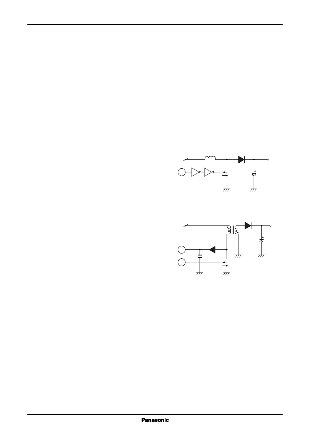
[2] Since the output 2 of the AN8018SA is assuming the bipolar transistor driving, it is necessary to pay attention to
the following points when directly driving n-channel MOSFET.
1. Select an n-channel MOSFET having a low input
capacitance
VIN
SBD
VOUT
The AN8018SA is of the constant-current (50 mA
maximum) output source-current type circuit assum-
ing the bipolar transistor driving. Also, its sink cur-
10
Out2
rent capability is around 80 mA maximum. For those
reason, it is necessary to pay attention to the increase
of loss due to the extension of the output rise time and
Figure 1. Output boost circuit example
the output fall time.
If any problem arises, there is a method to solve it
by amplifying with inverters as shown in figure 1.
VIN
SBD
VOUT
2. Select an n-channel MOSFET having a low gate
threshold value
The output high-level voltage of Out2 pin of the
AN8018SA is VCC −1.0 V minimum, so that it is
necessary to select a low VT MOSFET having a suffi-
ciently low on-state resistance in accordance with the
using operating supply voltage.
If a larger VGS is desired, there is a method to apply
the double-voltage of the input to the IC's VCC pin by
using the transformer as shown in figure 2.
VCC
SBD
9
10
Out2
VCC ≈ 2 × VIN − VD
Figure 2. Gate drive voltage increasing method
[3] In order to realize a low noise and high efficiency, a care should be taken in the following points in designing the
board layout.
1. The wiring for ground line should be taken as wide as possible and grounded separately from the power system.
2. The input filter capacitor should be arranged in a place as close to VCC and GND pin as possible so as not to
allow switching noise to enter into the IC inside.
3. The wiring between the Out terminal and switching device (transistor or MOSFET) should be as short as possible
to obtain a clean switching waveform.
4. In wiring the detection resistor of the output voltage, the wiring for the low impedance side should be longer.
[4] There is a case in which this IC does not start charging to the S.C.P. capacitor when the output is short-circuited
due to the malfunction of U.V.L.O. circuit biased by VCC that has ripples generated by turning on and off of the
switching transistor. The allowable range of the VCC ripple is as shown in the following figure. Reduce the VCC ripple
by inserting a capacitor near the VCC terminal and GND terminal of this IC so that the VCC ripple is in this allowable
range. However, this allowable range is design reference value and not the guaranteed value.
9
Share Link: