AN8018SA Ver la hoja de datos (PDF) - Panasonic Corporation
Número de pieza
componentes Descripción
Fabricante
AN8018SA
Panasonic Corporation

AN8018SA Datasheet PDF : 26 Pages
| |||
Voltage Regulators
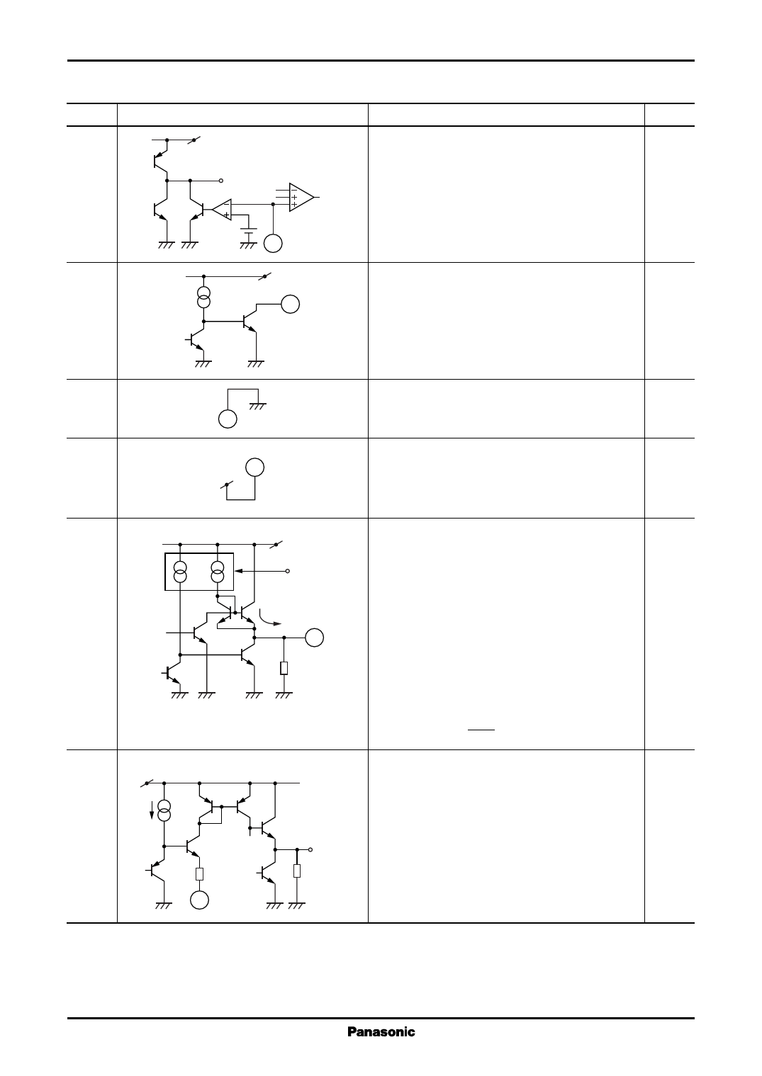
s Terminal Equivalent Circuits (continued)
Pin No.
Equivalent circuit
6
VCC
FB1 OSC PWM
0.2 V
6
7
VCC
7
AN8018SA
Description
I/O
DT1:
I
The pin for setting channel 1 output maximum
duty ratio.
If this terminal is set at a voltage of 0.20 V or less,
FB1 terminal becomes low-level voltage and the
protective function for channel 1 output short-
circuit will stop (Unlatch function).
Out1:
O
The pin is open-collector type output terminal.
The absolute maximum rating of output current is
+50 mA.
8
GND:
Grounding terminal
8
9
VCC:
9
The supply voltage application terminal
Use the operating supply voltage in the range of
1.8 V to 14 V.
10
Out2:
O
VCC
The pin is push-pull type output terminal.
RB2
The absolute maximum rating of output source
current is −50 mA.
ISO(OUT)
10
The absolute maximum rating of output sink cur-
rent is +80 mA.
A constant current output with less fluctuation
30 kΩ
with power supply voltage and dispersion can be
obtained by the resistor externally attached to RB2
pin.
ISO(OUT)2 = 68 ×
VRB2
RB2
[A]
11
VCC
RB2:
I
The pin for connecting a resistor for setting chan-
nel 2 output current.
Use a resistance value in the range of 180 Ω to 1.1
120 Ω
Out2
kΩ.
The terminal voltage is 0.36 V (at RB2 = 820 Ω).
11
7
Share Link: