AN8018SA Ver la hoja de datos (PDF) - Panasonic Corporation
Número de pieza
componentes Descripción
Fabricante
AN8018SA
Panasonic Corporation

AN8018SA Datasheet PDF : 26 Pages
| |||
AN8018SA
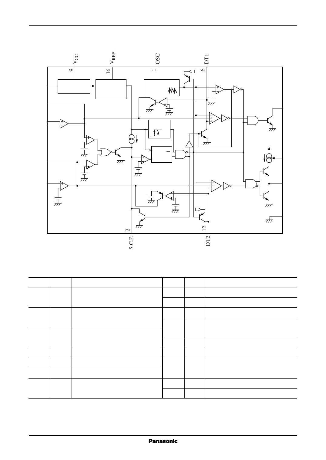
s Block Diagram
Voltage Regulators
On/ 15 On/off
off
control
FB1 5
Error amp. 1
IN−1 4
IN+1 3
FB2 13
0.9 V
Error amp. 2
IN+2 14
1.19 V
Reference 1.19 V
voltage source
Triangular wave
oscillation
VREF
VREF
0.9 V
S.C.P.
comp.
0.22 V
0.2 V
Unlatch1
U.V.L.O.
H
L
Latch
R
Q
S
VREF
PWM1
PWM2
0.9 V
Unlatch2
0.9 V
VREF
7 Out1
VCC
11 RB2
10 Out2
8 GND
s Pin Descriptions
Pin No. Symbol
Description
Pin No. Symbol
Description
1 OSC Pin for oscillation timing resistor
8 GND Grounding pin
and capacitor connection
9
VCC Power supply voltage application pin
2 S.C.P. Pin for connecting the time constant set- 10 Out2 Out2 block push-pull type output pin
ting capacitor for short-circuit protection 11 RB2 Out2 block output source current
3 IN+1 Error amplifier 1 block noninverting
setting resistor connection pin
input pin
12 DT2 PWM2 block dead-time setting pin
4 IN−1 Error amplifier 1 block inverting input pin 13 FB2 Output pin of error amplifier 2 block
5
FB1 Output pin of error amplifier 1 block 14 IN+2 Error amplifier 2 block inverting input
6
DT1 PWM1 block dead-time setting pin
pin
7 Out1 Out1 block open-collector type
output pin
15 Off On/off control pin
16 VREF Reference voltage output pin
2
Share Link: