AN725 Ver la hoja de datos (PDF) - Silicon Laboratories
Número de pieza
componentes Descripción
Fabricante
AN725 Datasheet PDF : 28 Pages
| |||

AN725
5.3. Low Power Mode Charge Pump
The SiM3L1xx devices feature a low-power, voltage-halving charge pump used to power most of the functions
operating in the lowest power mode (PM8). This charge pump always powers the low-frequency and 32 kHz crystal
oscillators. When in PM8, this charge pump also powers the following digital components: RTC counters and
alarms, LPTIMER0, UART0, ACCTR0, retention RAM banks, LCD0, and the Power Management Unit (PMU) and
reset controllers. When not in PM8, these modules are powered by the Memory regulator (LDO0). The analog
circuitry of the LCD and Pulse Counter is always powered directly from the VBAT pin.
The low power mode charge pump is a voltage-halving circuit which reduces the sleep-mode supply current using
two methods:
1. It provides approximately VBAT divided-by-2 to the oscillators and digital logic, reducing their inherent
power consumption.
2. It provides a transformer effect which causes the current pulled from the VBAT input to be ideally one-half
of the current actually consumed by the circuitry powered by the charge pump.
This charge pump can be modeled as a VBAT divided-by-2 supply with a series impedance of RCPLOAD.
Equation 1 shows the equation for the output voltage of the charge pump.
VCP
=
V-----B----A-----T--
2
–
ILOAD
RCPLOAD
Equation 1. Charge Pump Output Voltage
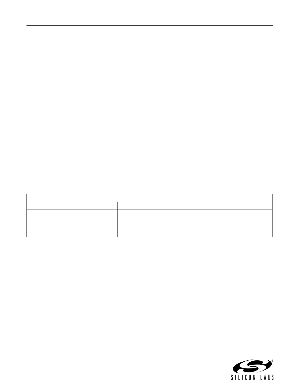
The value of RCPLOAD depends on the output drive setting field (CPLOAD) in the PMU module and the clock
selected by the RTC0 module, as shown in Table 3.
Table 3. Charge Pump Output Drive Settings
CPLOAD field
0
1
2
3
RCPLOAD Value
LFOSC (16.4 kHz) RTCOSC (32 kHz)
~600 k
~300 k
~200 k
~100 k
~90 k
~45 k
~40 k
~20 k
Overhead Current
LFOSC (16.4 kHz) RTCOSC (32 kHz)
~0 nA
~0 nA
~25 nA
~50 nA
~50 nA
~100 nA
~75 nA
~150 nA
All circuitry powered by the charge pump operates correctly at VCP voltages greater than or equal to 0.95 V. Thus,
for a given charge pump load current, Equation 2 must be true.
V-----B----A-----T--
2
–
ILOAD
RCPLOAD
0.95
V
Equation 2. Charge Pump Output Voltage Requirement
In all applications with a VBAT voltage of 2.4 V or above, the charge pump can operate at its minimum drive
impedance (CPLOAD = 3). However, as shown in Table 3, the overhead current consumed by the charge pump
increases as its drive impedance decreases. Therefore, at lower values of ILOAD, the total PM8 current
consumption can be reduced by increasing the charge pump’s drive impedance. In addition, since a higher drive
impedance corresponds to a lower output voltage for a given load current, increasing the drive impedance also
reduces the current consumed by the load circuitry.
At higher temperatures, using the low power charge pump and RTC0 can help reduce the leakage current of the
device. Reducing CPLOAD can further reduce the leakage at these temperatures.
18
Rev. 0.1