AN501 Ver la hoja de datos (PDF) - Vishay Semiconductors
Número de pieza
componentes Descripción
Fabricante
AN501 Datasheet PDF : 11 Pages
| |||
AN501
Vishay Siliconix
FSK
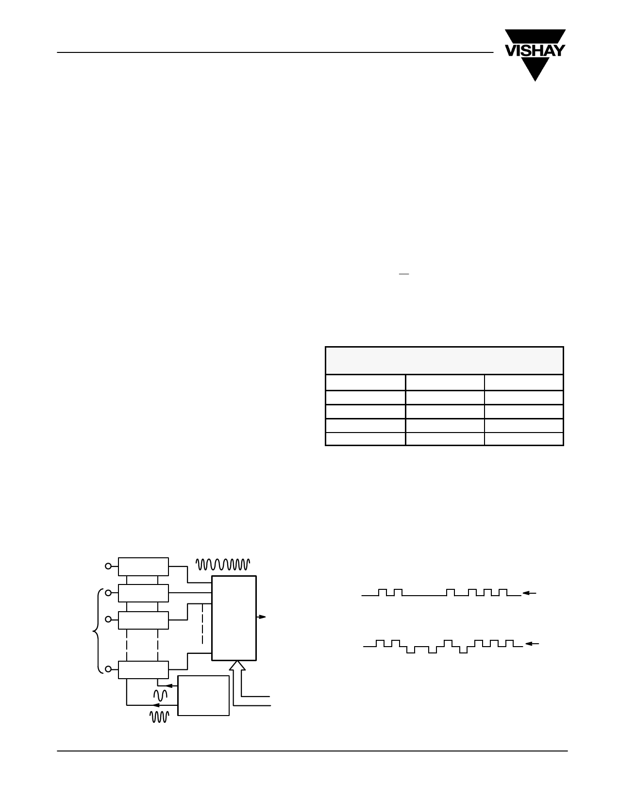
Frequency shift keying (FSK), commonly used in data
transmission networks, relies on representing the digital code
with frequency sine wave bursts. An FSK multiplexing system
block diagram is shown in Figure 14. Each digital level has a
specific signal frequency. The DG535/536 can be used to
multiplex 16 different digital channels into a single
transmission line or into a transmitter. Similarly, a DG535/536
may be used to demultiplex the data at the receiving end.
Since the device can manipulate higher frequency sine waves,
data can be transmitted at a higher rate than with a
conventional multiplexer.
PCM
A more commonly used and faster form of digital data
transmission is known as PCM (pulse coded modulation).
Used in telecommunications systems, PCM converts analog
speech signals into 8-bit digital words for serial transmission.
The data transfer rate used (for 4 kHz bandwidth voice signals)
is up to 274.176 Mbps.
The DG535/536 can be used to route PCM signals in main
telephone exchanges, replacing bulky hard-wired distribution
frames. PCM highways can thus be rerouted remotely, under
computer control, rather than manually.
RZ (returns to zero) PCM data consists of three discrete
(ternary) levels to overcome long periods of zeroes (Figure
13). Digital signals can degrade beyond legibility after only a
few hundred yards of travel down a transmission line.
Therefore, the PCM signals must be regenerated at regular
distances to avoid excessive distortion.
Figure 16 shows the architecture of a conventional binary
distribution frame in a telephone exchange. Signal
regeneration is applied to handle degradation during
transmission and routing. Code converters are required to
change the ternary PCM into binary PCM for routing within the
distribution frame. Similarly, code converters are required to
reconvert the binary PCM into ternary PCM for transmission.
Unlike digital switches which require specific digital signals,
using the DG535/536 in the distribution frame (Figure 17)
eliminates the need for code conversion and meticulous
regeneration because it can handle analog signals.
Programmable Gain Video Amplifier
The circuit shown in Figure 19 uses the DG536 as a binary
gain select for a video/wideband op-amp (CLC410).
The gain of the Si582 is set by:
AV
+
1
)
Rf
Rg
For example, listed below in Table 2 are the results when Rf
= 470 W.
TABLE 2.
Gains For The Circuit of Figure 19
Logic Input
0000
Rg
47 kW
Gain (AV)
1.0
0001
4.7 kW
1.1
0010
2.4 kW
1.2
0011
1.6 kW
1.3
The low on-resistance of the DG535/536 gives good gain
stability, and the resistor tolerances mainly determine the gain
error of the circuit.
The wideband qualities of the CLC410 allows this circuit to be
employed for digital level correction in any video systems
including broadest quality specifications.
e.g. 1011
Digital
Input
Channels
FSK
Generator
FSK
Generator
FSK
Generator
FSK Output
S1
S2 DG535/
S3 DG536
D
FSK
Generator
S16 A0 to A3
Output
to Transmission
Line or
Transmitter
Input
Stage
Frequency
(f0)
Synthesizer
(f1)
Address
Bus
FIGURE 14. FSK Multiplexing System Block Diagram
Binary
PCM
a) Analog voice signal converted to digital signal using
8 bits per sample
Ternary
PCM
b) Digital signal transmitted and clock regenerated
from digital signal to get synchronization
FIGURE 15.
www.vishay.com S FaxBack 408-970-5600
6-8
Document Number: 70608
03-Aug-99
Share Link: 