AN501 Ver la hoja de datos (PDF) - Vishay Semiconductors
Número de pieza
componentes Descripción
Fabricante
AN501 Datasheet PDF : 11 Pages
| |||
AN501
Vishay Siliconix
The DG536 is housed in a small, 44-pin J-lead package, thus
minimizing board size requirements. The DG535 is packaged in
a 28-pin DIP. Chip select pins (CS and CS) permit easy stacking
of devices for multi-channel multiplexing systems (see
Applications Section, Figure 19).
An additional feature, a DIS pin, is an open drain terminal with the
source tied to the device substrate. The DIS terminal represents
a high impedance to the substrate (normally ground) when the
DG535/536 is disabled and a low impedance to ground when the
DG535/536 is enabled. This output can be used to indicate which
device in a large matrix has been enabled (see Figure 13), or it
can be used to switch off circuitry following the multiplexer stages.
Two-Level Switching
The two-level switching system of the DG535/536 (SW4 and
SW5) works out of phase, effectively isolating half of the switch
outputs from the drain (output) of the multiplexer. These series
switches serve several functions:
They provide an extra stage of off-isolation.
They reduce the drain output capacitance significantly and
increase the multiplexing transition speed.
They reduce the off-leakage current, which reduces the offset
voltage that develops from the total off-leakage current flowing
through the load resistance and/or switch on-resistance. This
enables lower analog signal levels to be handled accurately.
Minimizing Parasitic Effects
The insertion loss and bandwidth of the switch are improved with
DMOS transistors that offer a low on-resistance and low intrinsic
capacitance (see Vishay Siliconix SD5000 data sheet). On the
DG536 channel-to-channel crosstalk is minimized by physically
separating each input channel with a GND pin which extends to
the device substrate. This, in conjunction with careful PC board
layout (see Figure 6), can yield channel-to-channel crosstalk
figures better than –92 dB at 5 MHz.
Further ac performance benefits are obtained through the
n-channel DMOS transistor T configurations (Figure 2). This
maximizes the off-isolation, since SW2 provides a shunt path to
ground for any signals fed through the parasitic capacitance
associated with SW1. SW3 (working in phase with SW1) provides
an extra stage of off-isolation and prevents the shunt switch
(SW2) from affecting consecutive channels.
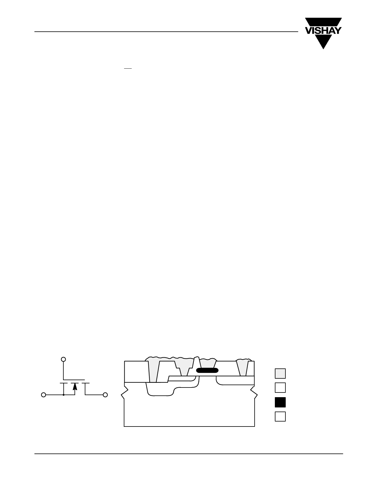
Silicon Gate
Polysilicon is used as the transistor gate material for the
DG535/536, as opposed to more conventional metal-gate
designs. This technology minimizes the charge coupling of the
control-logic signals to the switch output due to the self-aligning
properties of the process. Metal-gate technology relies on
photolithographically aligning the gate metal with the channel
diffusions, resulting in greater overlap tolerances.
As shown in Figure 3, a PN junction exists between the p-type
substrate and the n-type channel diffusions. This junction should
not become forward biased by the analog signal going more
negative than the substrate potential (normally ground).
Device damage could result from the current flow through the
forward biased substrate-channel junction, exceeding the
aluminum current handling capacity (i.e. 20 mA). Analog signal dc
biasing or offsetting the device power supplies can prevent this
problem. These methods are discussed in the applications
section of this paper (Figure 7 and Figure 8).
Gate
Source
Symbol
Drain
ÊÊÊÊÊÊÊÊÊÊÊÊSÊÊÊourcÊÊÊe/BodÉÉÉÉÊÊÊyn+ÉÉÉÉÊÊÊÉÉÉÉÊÊÊGÉÉÉÉÊÊÊate ÉÉÉÉÊÊÊÉÉÉÉÊÊÊnÉÉÉÉÊÊÊ+DraÊÊÊin ÊÊÊ
p+
— Aluminum
ÉÉÉÉ— Gate Oxide
p-Substrate
— Polysilicon
ÊÊÊÊ— Field Oxide
FIGURE 3. Cross-Section of an N-Channel, Silicon-Gate DMOS Transistor
www.vishay.com S FaxBack 408-970-5600
6-2
Document Number: 70608
03-Aug-99
Share Link: 