GTL2002 Ver la hoja de datos (PDF) - Philips Electronics
Número de pieza
componentes Descripción
Fabricante
GTL2002 Datasheet PDF : 24 Pages
| |||
When the GTL-TVC device is used as described in Figure 1, it is not necessary to have pull up resistors on the
lower voltage side because the GTL-TVC device will pass up to the reference Source voltage. With a 200 kΩ
resistor connected to the reference Drain (DREF) and the reference Gate (GREF) and pulled up to a supply
voltage that is at least 1.5 V higher than the reference Source (SREF) level, about 2.5 µA will pass to the
lower voltage side at the reference Source voltage value. If the low voltage side is known to be leaky (more than
the 2.5 µA described above), it is necessary to include a pull up resistor on the low voltage side as well as the
high voltage side to provide the required current value.
2. Down Translation
When doing down translation, since there is no driver on the lower voltage side, the higher voltage driver may
be either totem pole without any pull up resistor or open drain with a pull up resistor, and no resistor pull up is
needed on the low voltage side unless it has excessive leakage (more than the 2.5 µA described in the
paragraph above).
3. Up Translation
A pull up resistor is always required on the higher voltage side to get the full high level, since the GTL-TVC
device will only pass the reference source voltage as a high when doing a up translation. A full CMOS driver or
an open drain driver with or without a pull up resistor on the low voltage side may be used. The resistor values
must be chosen so as not to overload the pull down driver nor the 15 mA limit of the GTL-TVC devices.
4. Multiple Voltage Bi-Directional Translation
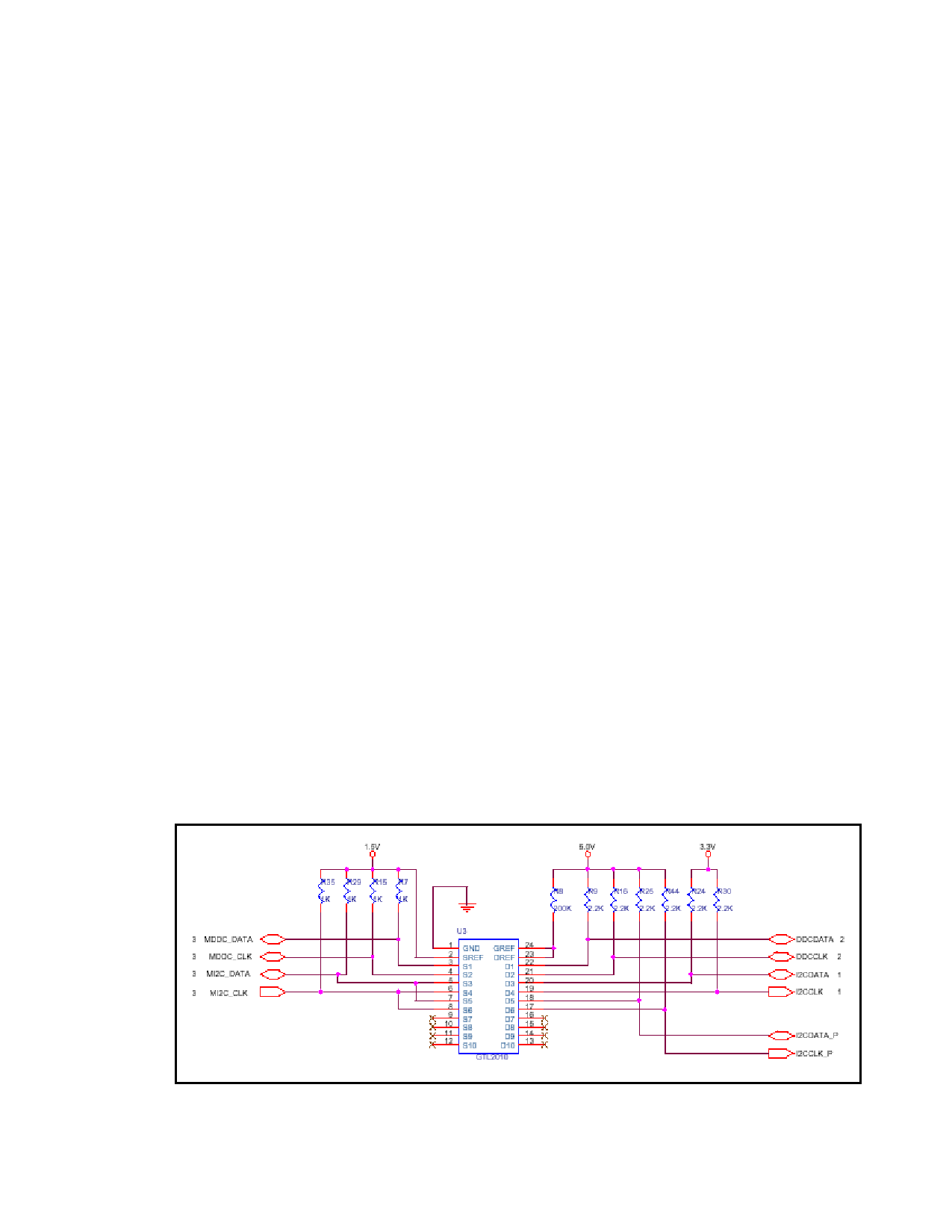
The channel pass transistors are constructed such that the gate of the reference transistor (GREF) pin is used to
limit the maximum high voltage that will be passed by the device. This allows the use of different bus voltages
on each source to drain channel so that for example, a 1.5 V device can communicate with 2.5 V, 3.3 V or 5 V
devices without any additional protection. Figure 2 shows how the GTL2010 can be used in a bi-directional I2C
application where two ASIC’s I2C ports (left side) operating at 1.5 V can interface to higher voltage devices
(right side) operating at 3.3V and 5.0 V.
- One of the ASIC ports (MDDC on S1 & S2) only needs to interface with 5 V I2C devices.
- The other ASIC port (MI2C on S3 & S4 and S5 & S6) needs to interface with both 3.3 V SMBus and 5.0 V
I2C devices.
Since the voltage difference between the low voltage (1.5V, left side) and the voltage on the resistor for the
GREF (Gate pull-up) is higher than 1.5V (5.0V in the figure), pull up resistors on the low voltage side (1.5V)
are optional.
Note:
Pull up resistors on the low voltage side are required if:
- Te difference between the external voltage applied on the resistor for the Gate reference (GREF) and
the voltage on the low side is lower than 1.5V
- The device in the low voltage side has a leakage current value higher than 2.5 µA
Figure 2. Bi-directional Multiple Voltage I2C Application
4
Share Link: 