IS61LPS51218D(2002) Ver la hoja de datos (PDF) - Integrated Silicon Solution
Número de pieza
componentes Descripción
Fabricante
IS61LPS51218D
(Rev.:2002)
(Rev.:2002)
Integrated Silicon Solution

IS61LPS51218D Datasheet PDF : 29 Pages
| |||
IS61LPS25632T/D/J, IS61LPS25636T/D/J, IS61LPS51218T/D/J
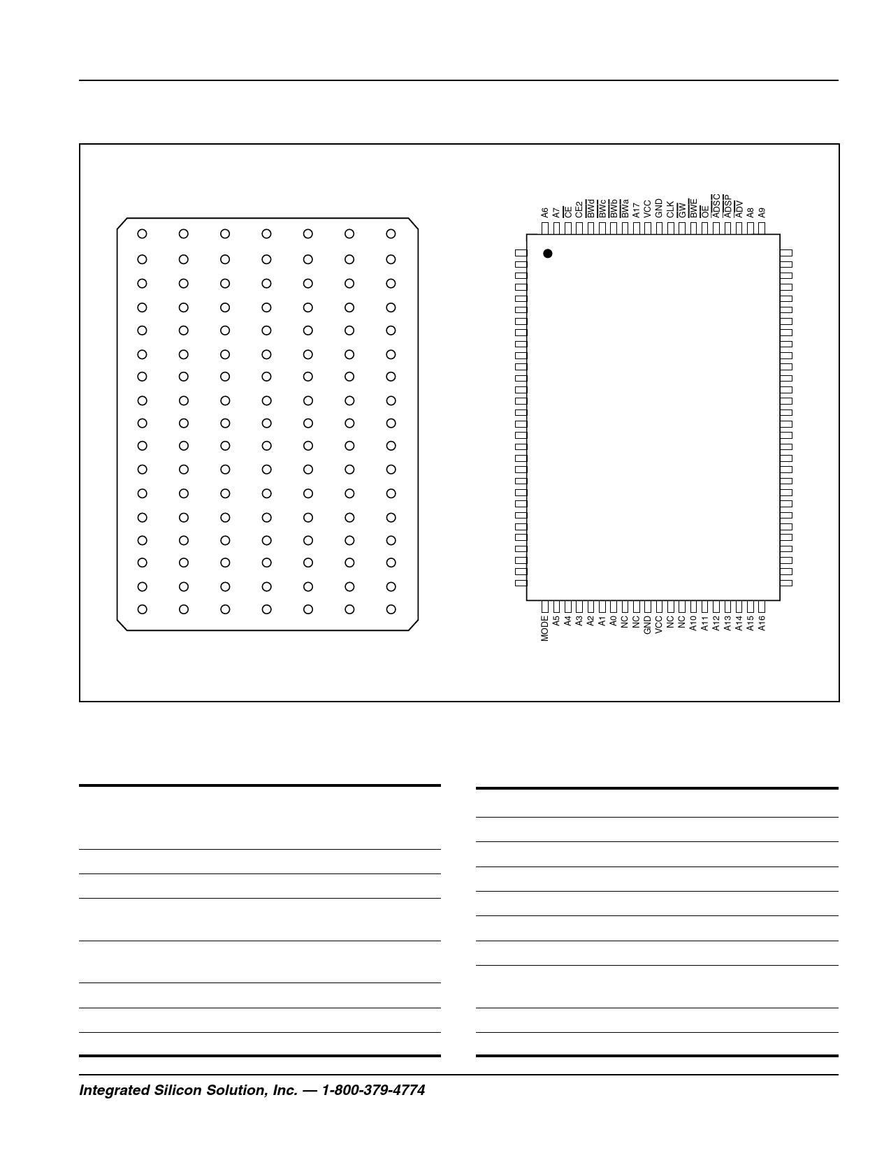
PIN CONFIGURATION
119-pin PBGA (D Version)
(Top View)
1
2
3
4
5
6
7
A
VCCQ
B
NC
C
NC
D
DQc
E
DQc
F
VCCQ
G
DQc
H
DQc
J
VCCQ
K
DQd
L
DQd
M
VCCQ
N
DQd
P
DQd
R
NC
T
NC
U
VCCQ
A
CE2
A
NC
DQc
DQc
DQc
DQc
VCC
DQd
DQd
DQd
DQd
NC
A
NC
NC
A
ADSP
A
ADSC
A
VCC
GND
GND
GND
BWc
NC
CE
OE
ADV
GND
GW
NC
VCC
GND
BWd
GND
CLK
NC
BWE
GND
A1
GND
A0
MODE VCC
A
A
NC
NC
A
A
A
GND
GND
GND
BWb
GND
NC
GND
BWa
GND
GND
GND
NC
A
NC
A
A
A
NC
DQb
DQb
DQb
DQb
VCC
DQa
DQa
DQa
DQa
NC
A
NC
NC
VCCQ
NC
NC
DQb
DQb
VCCQ
DQb
DQb
VCCQ
DQa
DQa
VCCQ
DQa
DQa
NC
ZZ
VCCQ
256K x 32
®
ISSI
PIN DESCRIPTIONS
A0, A1
A
CLK
ADSP
ADSC
ADV
BWa-BWd
BWE
Synchronous Address Inputs. These
pins must tied to the two LSBs of the
address bus.
Synchronous Address Inputs
Synchronous Clock
Synchronous Processor Address
Status
Synchronous Controller Address
Status
Synchronous Burst Address Advance
Individual Byte Write Enable
Synchronous Byte Write Enable
GW
Synchronous Global Write Enable
CE, CE2, CE2 Synchronous Chip Enable
OE
Output Enable
DQa-DQd
Synchronous Data Input/Output
MODE
Burst Sequence Mode Selection
VCC
+3.3V Power Supply
GND
Ground
VCCQ
Isolated Output Buffer Supply:
+3.3V or 2.5V
ZZ
Snooze Enable
DQPa-DQPd Parity Data I/O
Integrated Silicon Solution, Inc. — www.issi.com — 1-800-379-4774
3
PRELIMINARYINFORMATION Rev. 00B
04/29/02
Share Link: