M95128-WDL3T Ver la hoja de datos (PDF) - STMicroelectronics
Número de pieza
componentes Descripción
Fabricante
M95128-WDL3T Datasheet PDF : 20 Pages
| |||
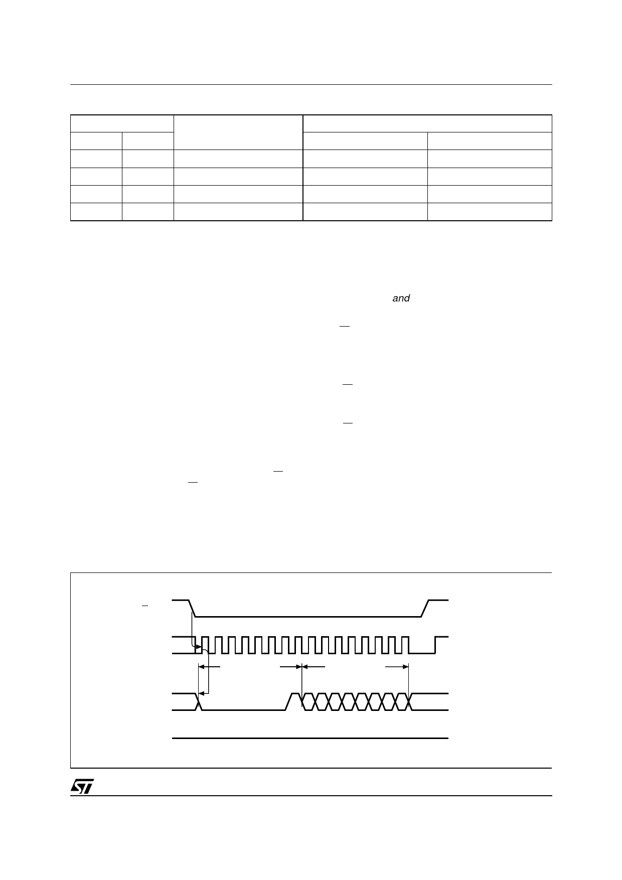
Table 6. Write Protected Block Size
Status Register Bits
BP1
BP0
Protected Block
0
0
none
0
1
Upper quarter
1
0
Upper half
1
1
Whole memory
M95256, M95128
Array Addresses Protected
M95256
M95128
none
none
6000h - 7FFFh
3000h - 3FFFh
4000h - 7FFFh
2000h - 3FFFh
0000h - 7FFFh
0000h - 3FFFh
The size of the write-protection area applies equal-
ly in SPM and HPM. The BP1 and BP0 bits of the
status register have the appropriate value (see Ta-
ble 6) written into them after the contents of the
protected area of the EEPROM have been written.
The initial delivery state of the BP1 and BP0 bits is
00, indicating a write-protection size of 0.
Software Protected Mode (SPM)
The act of writing a non-zero value to the BP1 and
BP0 bits causes the Software Protected Mode
(SPM) to be started. All attempts to write a byte or
page in the protected area are ignored, even if the
Write Enable Latch is set. However, writing is still
allowed in the unprotected area of the memory ar-
ray and to the SRWD, BP1 and BP0 bits of the sta-
tus register, provided that the WEL bit is first set.
Hardware Protected Mode (HPM)
The Hardware Protected Mode (HPM) offers a
higher level of protection, and can be selected by
setting the SRWD bit after pulling down the W pin
or by pulling down the W pin after setting the
SRWD bit. The SRWD is set by the WSR instruc-
tion, provided that the WEL bit is first set. The set-
ting of the SRWD bit can be made independently
of, or at the same time as, writing a new value to
the BP1 and BP0 bits.
Once the device is in the Hardware Protected
Mode, the data bytes in the protected area of the
memory array, and the content of the status regis-
ter, are write-protected. The only way to re-enable
writing new values to the status register is to pull
the W pin high. This cause the device to leave the
Hardware Protected Mode, and to revert to being
in the Software Protected Mode. (The value in the
BP1 and BP0 bits will not have been changed).
Further details of the operation of the Write Protect
pin (W) is given earlier, on page 3.
Typical Use of HPM and SPM
The W pin can be dynamically driven by an output
port of a microcontroller. It is also possible,
though, to connect it permanently to VSS (by a sol-
der connection, or through a pull-down resistor).
The manufacturer of such a printed circuit board
can take the memory device, still in its initial deliv-
ery state, and can solder it directly on to the board.
After power on, the microcontroller can be instruct-
ed to write the protected data into the appropriate
area of the memory. When it has finished, the ap-
propriate values are written to the BP1, BP0 and
Figure 8. WRSR: Write Status Register Sequence
S
0 1 2 3 4 5 6 7 8 9 10 11 12 13 14 15
C
INSTRUCTION
STATUS REG.
D
76543210
MSB
HIGH IMPEDANCE
Q
AI02282
7/20
Share Link: 