AIC1848 Ver la hoja de datos (PDF) - Analog Intergrations
Número de pieza
componentes Descripción
Fabricante
AIC1848 Datasheet PDF : 10 Pages
| |||
AIC1848
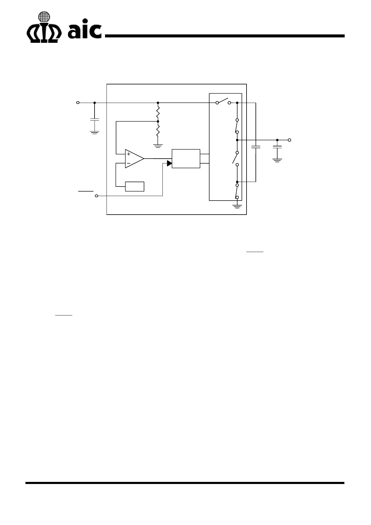
BLOCK DIAGRAM
VOUT
COUT
1µF
SHDN
COMP
VREF
Control
2
1
2
1
C+
CFLY
1µF
VIN
CIN
1µF
C-
PIN DESCRIPTIONS
PIN 1:VOUT -
Regulated output voltage. For the
best performance, VOUT should be
bypassed a 1µF (min.) low ESR
capacitor with the shortest
distance in between.
PIN 2: GND - Ground. Should be tied to ground
plane direct for best performance.
PIN 3: SHDN - Active low shutdown input. Tie to
higher than 1.4V to enable device,
0.3V or less to disable device.
APPLICATION INFORMATION
Introduction
AIC1848 is a micropower charge pump DC/DC
converter that produces a regulated 5V output
with an input voltage range from 2.7V to 4.5V. It
utilizes the charge pump topology to boost VIN to
a regulated output voltage. Regulation is obtained
by sensing the output voltage through an internal
resistor divider. A switched doubling circuit
enables the charge pump when the feedback
voltage is lower than the internal comparator point,
and vice versa. When the charge pump is enabled,
a two-phase non-overlapping clock activates the
SHDN pin is not allowed to float.
PIN 4: C- - Flying capacitor negative terminal.
PIN 5: VIN - Input supply voltage. VIN should
be bypassed a 1µF (min.) low
ESR capacitor with the shortest
distance in between.
PIN 6: C+ - Flying capacitor positive terminal.
charge pump switches.
Operation
This kind of converter uses capacitors to store
and transfer energy. Since the capacitors can’t
change to the voltage level abruptly, the voltage
ratio of VOUT to VIN is limited. Capacitive voltage
conversion is obtained by switching a capacitor
periodically. Refer to Fig. 11, during the on state
of internal clock, Q1 and Q4 are closed, which
charges CFLY to VIN level. During the off state, Q3
and Q2 are closed. The output voltage is VIN plus
6
Share Link: 