M95256-BN1 Ver la hoja de datos (PDF) - STMicroelectronics
Número de pieza
componentes Descripción
Fabricante
M95256-BN1 Datasheet PDF : 21 Pages
| |||
M95256, M95128
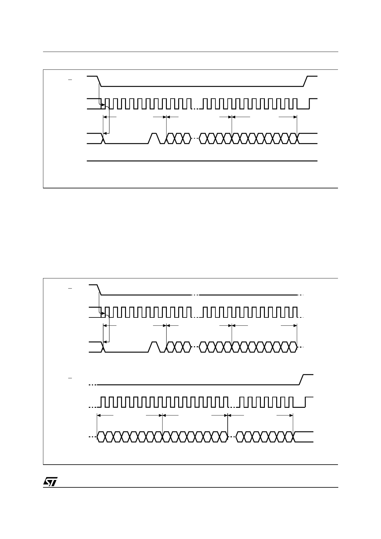
Figure 11. Byte Write Operation Sequence
S
0 1 2 3 4 5 6 7 8 9 10 20 21 22 23 24 25 26 27 28 29 30 31
C
INSTRUCTION
16 BIT ADDRESS
DATA BYTE
D
15 14 13 3 2 1 0 7 6 5 4 3 2 1 0
HIGH IMPEDANCE
Q
Note: 1. Depending on the memory size, as shown in Table 7, the most significant address bits are Don’t Care.
AI01795
next address, can be read by successive clock
pulses. When the highest address is reached, the
address counter rolls over to “0000h”, allowing the
read cycle to be continued indefinitely. The read
operation is terminated by deselecting the chip.
The chip can be deselected at any time during
data output. If a read instruction is received during
a write cycle, it is rejected, and the memory device
deselects itself.
Byte Write Operation
Before any write can take place, the WEL bit must
be set, using the WREN instruction. The write
state is entered by selecting the chip, issuing three
Figure 12. Page Write Operation Sequence
S
0 1 2 3 4 5 6 7 8 9 10 20 21 22 23 24 25 26 27 28 29 30 31
C
INSTRUCTION
16 BIT ADDRESS
DATA BYTE 1
D
15 14 13 3 2 1 0 7 6 5 4 3 2 1 0
S
32 33 34 35 36 37 38 39 40 41 42 43 44 45 46 47
C
DATA BYTE 2
DATA BYTE 3
DATA BYTE N
D
7654321076543210
6543210
Note: 1. Depending on the memory size, as shown in Table 7, the most significant address bits are Don’t Care.
AI01796
9/21
Share Link: 